|
|
Burn-in & Test
Socket WorkshopTM |
|
|
|
BiTS Home
Archive
Committee
Subscribe
Links |
|
BiTS
is the world's premier workshop dedicated to
providing a forum for the latest information
about burn-in and test socketing, and related
fields.
At BiTS you'll find a comprehensive technical
program, exhibits of the latest products and
services, and many opportunities to meet,
network and explore ideas with other test and
burn-in socketing professionals.
Click here if you need the latest Acrobat(R) reader
from Adobe(R):

or
for an alternate free PDF
viewer, download the latest
Sumatra PDF
It is FAST! |
|
|
 |
ARCHIVE PAGES |
|
|
COPYRIGHT NOTICE |
|
The papers in this publication
comprise the proceedings of the 2006 BiTS Workshop. They reflect the authors’
opinions and are reproduced as presented , without change. Their inclusion in
this publication does not constitute an endorsement by the BiTS Workshop, the
sponsors, BiTS Workshop LLC, or the authors.
There is NO copyright protection claimed by this publication or the authors.
However, each presentation is the work of the authors and their respective
companies: as such, it is strongly suggested that any use reflect proper
acknowledgement to the appropriate source. Any questions regarding the use of
any materials presented should be directed to the author/s or their companies.
All photographs on this page are copyrighted by BiTS Workshop LLC. The BiTS logo
and ‘Burn-in & Test Socket Workshop’ are trademarks of BiTS Workshop LLC.
|
|
|
|
Background
|
|
BiTS Workshop 2006 brought together over 350 attendees and
more than 50 exhibitors from around the world representing end users and
suppliers of sockets, boards, burn-in systems, handlers, packages and other
related equipment, materials and services.
|
|
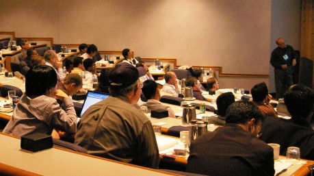
Technical Program
|
|
More than 25 presentations
addressing important topics in socketing and related areas were delivered by authors from the user and supplier communities.
Three Tutorials
were offered where participants learned from experts to build your
leading edge skills.
In the keynote
address, a renowned industry leader spoke on a key
topic sure to stimulate thoughts and ideas.
Our panel discussion
brought together a distinguished group of experts who shared their thoughts and take questions on a challenging subject of
current interest.
|
|
|
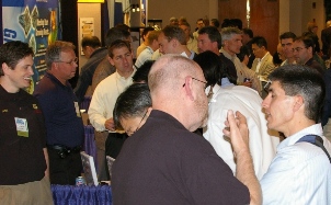
BiTS 2006 Expo
|
|
Over 50 exhibitors, from
socketing and related industries, exhibited their products
during breaks in the technical program.
Click HERE for a directory of
exhibitors.
|
|
|
BiTS 2006 Attendees
|
|
Over 350 workshop attendees from all over the world
participated in BiTS 2006.
|
|
BiTS 2006 in the Press
|
|
|
|
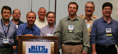
BiTS 2006 Organizing Committee
|
|
Valts Treibergs (Everett Charles Technologies), Marc Paul Boyce (Advantage Specialist),
Mike Noel (Freescale), Steve Hamren (Micron Technology), Fred Taber (BiTS
Workshop), Owen Prillaman (Yamaichi Electronics). Not pictured: Mark
Murdza (UMD Advanced Test Technologies), John Ambrosini (Enplas-Tesco)
|
|
|
|
|
BiTS
TUTORIALS 2006 |
|
Tutorial 1 |
Fundamental
Properties of Electrical Contacts |
2006tutorial_timsit.pdf
 (214 KB)
|
|
 |
|
Dr. Roland Timsit, President
Timron Scientific Consulting Inc. |
|
| Do you
know the source of "contact resistance" ("cres")
in an electrical connection? Are you aware that a large number of
physical mechanisms, other than the passage of electrons, are
activated when you pass a current through an electrical junction?
Some of these mechanisms are detrimental to the life of the
contact. Why does a contact interface generally wear-off over
time, often caused by a so-called fretting mechanism? What
actually happens to cause interfacial heating in the contact? Why
do we see changes in the composition of materials in a contact
interface under load? These questions and many other fundamental
properties of contacts, as well as how these properties apply
specifically to socket contacts, were addressed at this
tutorial. |
|
|
Tutorial 2 |
Differential
Impedance And Insertion Loss Applied To Test Sockets |
2006tutorial_bogatin.pdf
(795 KB)
|
|

|
|
Dr. Eric Bogatin, CTO
Synergetix |
|
| This
tutorial built on last year's tutorial ("Signal
Integrity of Test Sockets - Simplified!") by focusing on two
major topics, single and differential impedance and making sense
of insertion and return loss. The impedance discussion helped
the attendee understand how single-ended impedance and
differential impedance differ and how each are used in test
hardware design. The second half of the tutorial focused on the
frequency based specifications of insertion and return loss.
Discussions on how the two parameters work to define hardware
(i.e. sockets) targets were examined. The session concluded
with a practical look at some real world measurements of sockets
in the frequency domain. |
|
|
Tutorial 3 |
Geometric
Dimensioning and Tolerancing: A Primer for the BiTS Professional |
2006tutorial_allsup.pdf
(588 KB)
|
|

|
|
Thomas Allsup,
Manager of Technology Anida Technologies |
|
| This
tutorial was directed at users and creators of mechanical drawings
by covering proper dimensioning and tolerances based on the ASME
Y14.5M-1994 standard. The tutorial highlighted proper use of
Form, Orientation, Profile, Runout, and Location and provided
helpful, handy guidelines for their application. This tutorial was
kept interactive with numerous examples for the student to
practice the topics during the course. |
|
|
| Panel
Discussion |
Thinner
Packages and PoP Present Real Challenges for Test & Burn-in |
2006panel.pdf
(214 KB)
|
Preface:
Cell phones, PDAs and other handheld devices are driving maximum
functionality in the smallest footprint and lowest profile at the lowest
cost. The resulting trend is toward extremely thin packages - less than
.5mm - to support stacking processes, with fine pitch and solder bumps or
LGA pads. This leads the socket supplier to offer vertical compression
contact systems with their accompanying high clamping forces. Adding
temperature further increases the potential for package warping. How is a
socket to handle such challenges?
Abstract:
Panelists representing semiconductor and equipment supplier sectors
discussed the challenges presented by these thinner packages and the drive
toward small outline, open top sockets that can be automated to achieve
low cost burn-in. They explored, share and debate ideas for socket
solutions; along with discussing industry acceptable / allowable package
deformation / stress and best practices that the industry can adopt to
mitigate the challenges of such thin packages/dies.
Panel Members:
| Prasanth Ambady |
Texas Instruments IBU |
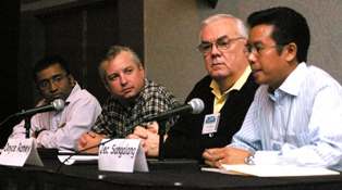
|
| Kent Carrie |
Amkor |
| Doyce Ramey |
Texas Instruments S/C |
| Jec Sangalang |
Yamaichi Electronics USA |
|
|
|
BiTS
2006 TECHNICAL PROGRAM - SESSIONS
Covering the Latest Information on Important
Topics in Socketing and Related Areas |
|
DESIGN DAY |
| Opening
Remarks |
|
2006welcome.pdf
(518 KB) |
| Welcoming remarks from the General
Chair. |
|
Session 1 |
Advanced Socket Materials |
2006s1.pdf
(2.46 MB)
|
| With
requirements like high temperature, chemical resistance and ESD
compatibility, sockets are a demanding application for materials. This
session explored materials used for socket housings that address these
requirements, and took a look at materials where high insertion
life and dimensional stability requirements must be satisfied. |
|
"Carbon Nanotube
Polymer Composites for Socket Applications" |
Mark Hyman
Hyperion Catalysis Int'l, Inc. |
Tim Jozokos
Hyperion Catalysis Int'l, Inc. |
Yuanheng Zhang
Hyperion Catalysis Int'l, Inc. |
Heidi Sardinha
Hyperion Catalysis Int'l, Inc. |
|
|
| "PEEK-based
Solutions for Test Socket Applications" |
John Walling
Victrex USA, Inc. |
Sam Brahmbhatt
Victrex USA, Inc. |
|
| "Para-phenylene
Rigid Rod Polymers and Their Unique Attributes for Burn-in and
Test Sockets" |
Lorenzo P. DiSano
Ensinger Industries, Inc. |
|
|
|
|
Session 2 |
Socket
Design and Performance |
2006s2.pdf
(1.14 MB)
|
| With the ever pressing forces
of fine pitch requirements, and the never ending need to control costs,
socket design and performance are constantly being pushed to the edge.
This session explored socket performance over time, socket re-use
potential, and finally discussed some technologies that are enabling pitches
down to 0.3mm. |
| "Innovative Socket Technology
for 0.3mm Pitch BGA Devices" |
Ila Pal
Ironwood Electronics, Inc. |
|
|
|
"Socket
Performance Over Time and Insertion Count With Pb-Free
Applications"
 AWARD
WINNER AWARD
WINNER
|
Jeff Sherry
Johnstech International Corp. |
Bert Brost
Johnstech International Corp. |
|
| "A Case for Socket
Reuse - An Approach to Managing the Cost of High-End Burn-In
Sockets" |
Paul Gaschke
IBM Systems and Tech. Group |
Dave Carpentier
IBM Systems and Tech. Group |
|
|
|
Session 3 |
Electrical Analysis and Characterization |
2006s3.pdf
(2.58 MB) |
| Today's sockets are expected
to deliver power and signaling beyond customer's expectations while in
their harsh environment. To ensure the socket performs well, great effort
is invested by the customers, suppliers and specialized measurement firms
to best understand the sockets' attributes. This session focused on the
results of these specialized analyses showing just how in-depth one must
go to extract the optimal performance from a socket. |
| "Development of Computational
Model and Measurement of Maximum Current Capability for
Microprocessor Sockets" |
David W. Song
Intel Corporation |
Ashish Gupta
Intel Corporation |
Chia-Pin Chiu
Intel Corporation |
| "Lumped and
Distributed Equivalent Circuits for Test Sockets" |
Gert Hohenwarter
GateWave Northern, Inc. |
|
|
| "Contactor Characterization of
RF Test/Burn In" |
Ling Li Ong
Intel Corporation |
Tim Swettlen
Intel Corporation |
|
| "Differential Impedance
Characterization of Test Sockets" |
Eric Bogatin
Synergetix |
Kevin DeFord
Synergetix |
Meena Nagappan
Synergetix |
|
|
|
CHALLENGES
DAY |
|
Session 4 |
Managing
Advanced Packaging Demands |
2006s4.pdf
(5.44 MB)
|
| Keeping pace with the
Packaging Industry's ever escalating requirements for unique applications,
finer pitch and higher speeds presents a formidable hurdle to Test &
Burn-in tooling. This session captured the impact and offers innovative
solutions to the challenges and considerations driven by advanced
packaging and device operational demands. |
| "The Challenges of Handling
& Socketing Packaged Image Sensors" |
Steve Hamren
Micron Technology |
|
|
| "Ultra Fine Pitch
Socket Development Challenges" |
Wei-ming Chi
Intel Corporation |
Ken Kassa
Intel Corporation |
Chak Fung Kon
Intel Corporation |
| "PCB's In The
Test Environment" |
Hardeep Heer
Everett Charles Technologies STG |
"Are Sockets Required for Test
and Burn-in?"
 AWARD
WINNER AWARD
WINNER |
Belgacem Haba, Ph.D.
Tessera, Inc. |
|
|
|
|
Session 5 |
High Frequency Design and Measurement Considerations |
2006s5.pdf
(1.76 MB)
|
| Higher bandwidth devices
require more focus on the socket's physical structure and how it impacts
electrical performance. This session included both how these physical
structures impact electrical performance as well as how some suppliers
measure these attributes. |
| “Properties of Electrical Contacts
at High Frequencies” |
Roland S. Timsit, Ph.D., PE
Timron Scientific Consulting Inc. |
|
|
| “Accuracy
Improvements in Microwave Measurements by Double-Sided Probing” |
Habib Kilicaslan
Kulicke & Soffa Industries |
Bahadir Tunaboylu
Kulicke & Soffa Industries |
David McDevitt
Kulicke & Soffa Industries |
| “Effects of the Launch on
Bandwidth” |
Ryan Satrom
Everett Charles Technologies - STG |
|
|
|
|
Session 6 |
Interfacing: Contacting the Device and Beyond |
2006s6.pdf
(4.24 MB)
|
| Sometimes contacting the
device is only half the battle. The presenters discussed new challenges
for getting the device into the socket and then solutions to get clean
test signals to & from the tester. |
| "Comparison of Test
Interface Unit for High Frequency Applications (Comparison of
Coaxial Socket with Brass Body and Plastic Socket)" |
Takuto Yoshida
Yokowo Co., Ltd. |
Doyce Ramey
Texas Instruments, Inc. |
Jimmy Vo
Texas Instruments, Inc. |
| "Improving Test
Efficiency by New Device Interface Topology for High Parallel
Testing" |
Joachim Moerbt
Advantest (Europe) GmbH |
Rose Hu
Advantest (Europe) GmbH |
|
"Socketing the
Impossible: a Very Fine, Very Dense Case Study"
 AWARD
WINNER AWARD
WINNER |
Jon Diller
Synergetix |
Kiley Beard
Synergetix |
Takuya Tsumoto
NEC Electronics Japan |
|
|
Hot Topics Session |
A Trio of Trends and Challenges |
2006ht.pdf
(1.1 MB)
|
| This session focused on
emerging major trends/challenges, this is about the latest work on a trio of
them: test handling of advanced device packages, socket/board design for
high frequency/power and thermal non-uniformities. Each presenter
discussed their novel approach to one of these three trends/challenges and
provided an insight into a solution. |
| "Test Handling Challenges
Associated with Socket Designs" |
John Pollock
Aetrium Incorporated |
|
|
| "Optimization of
Interconnects" |
Ho Peng Ching
Micron Semiconductor Asia |
|
|
| "Thermal Considerations in
Testing Very High Performance Devices" |
Thomas Di Stefano
Centipede Systems |
|
|
|
|
|
BiTS 2006
KEYNOTE ADDRESS
|
2006keynote.pdf
(780 KB)
|
|
Test and
Burn-in: The World Beyond Scaling
|
|

Mr. Harris is the Worldwide Test Engineering
Manager for IBM's Systems and Technology group where he is responsible for
development and manufacturing Test and Burn-in engineering for all
semiconductor products manufactured by IBM, for IBM Systems group as well as
a variety of OEM customers.
|
John Harris
Manager, WW Test Engineering, IBM Systems & Technology Group
|
| As the semiconductor industry moves
into the post scaling era and arguably toward maturation, it is
faced with unique technical and economic challenges, many of which
will have significant ramifications on Test and Burn-in. Even in
the post scaling era, the server and network infrastructure
businesses will continue to drive performance and integration
levels for processors and ASIC's/SOC's which will push the limits
of Test and Burn-in technology.
Particularly challenging are the
microprocessors and graphics chips used in high end gaming
systems, which are amongst the most complex chips in the world and
yet must meet the cost objectives of the consumer, not the high
end, marketplace. In the storage, wireless and consumer
electronics markets the focus on cost will become ever more
intense and pervasive across all product types as a function of
"technology saturation" and growth into developing
markets.
In the midst of all this, the role of Test and Burn-in
has fundamentally changed from being primarily a process to sort
good die from bad to being a primary source of data feedback and
analysis for the wafer fab and design teams. Meeting the often
divergent needs of these various products and markets, as well as
the data collection needs, will especially challenge the Test and
Burn-in communities as they lack the cost leverage the wafer fabs
gain by moving to larger wafer and smaller die sizes. How we step
up to these challenges will be critical to the success of the
semiconductor industry in this new era.
|
|
|
|
PROCESS
DAY |
|
Session 7 |
Thermal Management Advances |
2006s7.pdf
(3.23 MB)
|
| Back again! Thermal challenges
are not going away, but our authors are taking the issue head on. This
session began with an overview of the thermal challenges associated
with Burn-in, and explored some innovative ways of addressing these
challenges. |
| "DUT Thermal
Management - An Overview of Applied Passive Thermal Control
Technology for Integrated Circuit Test" |
F. D. Boatright
Delta Design, Inc. |
|
|
| "Thermal Control
Units: Development of an Analytical Model and Experimental
Validation to Optimize the Voltage Input" |
Sudhir Kumar
Kulicke & Soffa Industries |
Khaled Elmadbouly
Kulicke & Soffa Industries |
Praba Prabakaran
Kulicke & Soffa Industries |
"Using a High
Performance Micro-channel Cold Plate for Test and Burn-in"
 AWARD
WINNER AWARD
WINNER |
Zahed Sheikh
Mikros Technologies |
|
|
| "Managing the
Thermal Budget During Burn-in - A New Concept for Control" |
Chris Lopez
UMD |
Dr. James Forster
UMD |
Trevor Moody
UMD |
|
|
Session 8 |
Test
and Burn-in Efficiency Initiatives |
2006s8.pdf
(1.68 MB)
|
| Efficiency! Everyone is
looking to lowers costs and improve manufacturing processes. This group of
papers encompassed a number of initiatives to improve the efficiency of a
variety of processes involving Test and Burn-in. |
| "Enabling High
Volume Testing of MCP Memory" |
Ken Karklin
Agilent Technologies |
|
|
| "An Alternative Test for
Verifying Connectivity on High Pin Count Devices During
Burn-in" |
Rick Larson, PE
Texas Instruments Inc. |
Bunny Gaab
Enplas Tesco, Inc. |
|
| "Minimizing Spring Probe
Operational Cost Using Optimized Maintenance Techniques" |
Erik Orwoll
Nu Signal LLC |
|
|
|
| Supplemental
Presentations |
Bonus
Presentations |
2006sup.pdf
(953 KB)
|
| BiTS
Workshop attendees were treated to a bonus of two fine supplemental papers
that were submitted as backup presentations. Thank you, authors and
presenters, for the extra effort! |
| "Sources
Of Variation And Error In Finite Element Analysis" |
Mike Gedeon
Brush Wellman, Inc. |
|
|
| "Cost
& Performance Optimization Of Air-cooled Burn-in Socket
Thermal Design” |
Hongfei Yan
Intel Corporation |
|
|
|
|
|
Page last modified
03/28/11
|
 |
BiTS WorkshopTM is a production of
BiTS Workshop LLC |
|