|
|
Burn-in & Test
Socket WorkshopTM |
|
|
|
BiTS Home
Archive
Committee
Subscribe
Links |
|
BiTS
is the world's premier workshop dedicated to
providing a forum for the latest information
about burn-in and test socketing, and related
fields.
At BiTS you'll find a comprehensive technical
program, exhibits of the latest products and
services, and many opportunities to meet,
network and explore ideas with other test and
burn-in socketing professionals.
Click here if you need the latest Acrobat(R) reader
from Adobe(R):

or
for an alternate free PDF
viewer, download the latest
Sumatra PDF
It is FAST! |
|
|
 |
ARCHIVE PAGES |
|
|
COPYRIGHT NOTICE |
|
The papers in this publication
comprise the proceedings of the 2008 BiTS Workshop. They reflect the authors’
opinions and are reproduced as presented , without change. Their inclusion in
this publication does not constitute an endorsement by the BiTS Workshop, the
sponsors, BiTS Workshop LLC, or the authors.
There is NO copyright protection claimed by this publication or the authors.
However, each presentation is the work of the authors and their respective
companies: as such, it is strongly suggested that any use reflect proper
acknowledgement to the appropriate source. Any questions regarding the use of
any materials presented should be directed to the author/s or their companies.
All photographs on this page are copyrighted by BiTS Workshop LLC. The BiTS logo
and ‘Burn-in & Test Socket Workshop’ are trademarks of BiTS Workshop LLC.
|
|
|
|
Technical Program
|
|
More than 25
presentations addressing important topics in socketing and related
areas were delivered by authors from the user and supplier communities.
INTRODUCING - Two Poster Sessions, where
attendees and authors communicated directly and interactively to share
and explore ideas.
Two Tutorials were offered
where participants learned from experts to build your leading edge skills.
A respected Invited Speaker
shared his views on advanced packaging trends and challenges.
In the Keynote Address, a renowned
industry leader spoke on a key topic sure to stimulate thoughts and
ideas.
|
|
BiTS EXPO
2008 |
| 60 exhibitors, from
socketing and related industries, exhibited their products and services
during breaks in the technical program. Click HERE for more
info on BiTS EXPO 2008. |
| Participants |
|
BiTS 2008 brought together 350 full-conference attendees and 60 exhibitors from
around the world, representing end users and suppliers of sockets, boards,
burn-in systems, handlers, packages and other related equipment, materials and
services.
|
|
BiTS 2008 in the Press
|
|
|
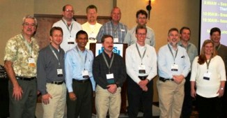
| BiTS
2008 Organizing Committee
|
Front:
Fred Taber (BiTS
Workshop), Morten Jensen (Intel), Rafiq Hussain (AMD), Mike Noel (Freescale),
Joachim Moerbt (Advantest Europe), John Moore (Texas Instruments), Steve Hamren (Micron Technology),
Kena Pegram (Anestel), Owen Prillaman (Yamaichi Electronics)
Back:
Marc Knox (IBM), Mark
Murdza (Cascade Microtech), Paul Boyce (Advantage Specialist), Valts Treibergs (Everett Charles
Technologies) |
 |
|
|
|
TUTORIAL
DAY
Sunday, March 9, 2008 |
|
Tutorial 1 |
Basic
Chip Reliability Concepts
(Product RE "101") |
2008tutorial1_swift.pdf
 (2.6 MB)
|
|
|
|
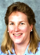
Ann Swift
Senior Engineer
IBM Microelectronics |
|
| This
talk focuses on the basic concepts of CMOS semiconductor
screening and failure rate projections. Basic reliability
engineering concepts are discussed (the "bathtub"
curve, the difference between wearout and defect mechanisms,
acceleration factors, etc.). Failure rate models to relate
accelerated testing/stressing to product lifetimes are illustrated. Various manufacturing screens (such as Burn-in and
Voltage Screen) are shown along with their impact on product
failure rates. What the future might hold for reliability
screening is also discussed. |
Who should
have attended this tutorial?
What is that accelerated testing/stressing that companies do using the sockets
developed by BiTS member companies? Have you ever wondered what these product
reliability engineers you talk to do? If so, this tutorial will help you
understand the world of reliability engineering and accelerated
testing/stressing. This talk will focus on basic concepts of CMOS semiconductor
screening and failure rate projections. Various manufacturing screens (such as
Burn-in and Voltage Screen) will be discussed along with their impact on product
failure rates. The talk will begin with the basic concepts of reliability
engineering. The differences between wearout and defect mechanisms in
semiconductor devices will be discussed. Reliability testing methods including
stress acceleration and screening will be illustrated and examples of how to
relate accelerated data to "real life" will be discussed. This
tutorial is a must for anyone interested in starting to understand the field of
chip reliability. |
|
|
Tutorial 2 |
Intellectual Property: What Is It and What Do I Do With It? |
2008tutorial2_blecker.pdf
(825 KB) |
|
|
|
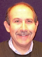
Ira Blecker, Esq.
Patent Attorney
Law Offices of Ira D. Blecker, P.C. |
|
| Intellectual
Property is important, and will become increasingly important, to
the electronics industry. Intellectual Property includes (but is
not limited to) patents, copyrights, trademarks and trade secrets.
After a brief review of the types of Intellectual Property, this
tutorial primarily focus on a deep dive into the patent
aspect of Intellectual Property. Topics included are pre-patent protection of your Intellectual Property, what is a
patent, how to read a patent, how to interpret the claims of a
patent, the patenting process from invention disclosure to patent,
types of patent applications, worldwide patenting mechanisms
including the Paris Convention, the European Patent Convention and
the Patent Cooperation Treaty and some recent important court
decisions. Patent enforcement, highlighting some troublesome
countries, are also be touched upon. |
Who should
have attended this tutorial?
Have you ever had questions on Intellectual Property but you didn't know who to
ask for answers? Have you ever wanted to learn more about Intellectual Property?
This tutorial is meant to be a primer on Intellectual Property for inventors,
engineers and business persons (i.e., specifically non-lawyers) who deal with
Intellectual Property in some way, shape or form. The tutorial will cover a
broad range of topics beginning with a definition of what is Intellectual
Property and then move into the arena of patents as Intellectual Property. The
tutorial will finish with some discussion of international aspects of protecting
and enforcing Intellectual Property. There will be something in the tutorial for
all those interested in the subject of Intellectual Property, whether you know a
little or a lot about Intellectual Property. |
|
|
| Invited
Speaker |
Catching
the Mobile Wave: Packaging is Going 3D |
2008invited_haba.pdf
(1.9 MB) |
|
|
|
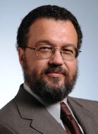
Dr. Belgacem Haba
Fellow and CTO of Advanced Packaging and Interconnect
Tessera Inc. |
|
|
|
Hand-held communication and entertainment products will
continue to dominate the consumer markets worldwide, and with each generation
offering more and more features and/or capability, system level integration and
miniaturization becomes more of a priority. And even though the actual
applications and functionality of the new product offering expands, the customer
is expecting each generation to be smaller and lighter that its predecessor.
The cell phone is a great example of how new technologies
and techniques can be applied to maintain performance improvements over time.
The explosion of the cell phone market over the last few years is a testament to
the increase of functionality and complexity of miniaturization. However, this has
led to some serious issues, especially mechanical, thermal and shielding
problems. Less than one part in 1,000 of the volume of an electronic product is
occupied by transistors. The remaining volume consists of mechanical structure,
air, passive elements, cables and connectors. 3D stacking is a natural way to
reduce the system volume. Die fabricated at different process geometries can be
brought together in a 3D stack, thus avoiding some of the cost issues associated
with system-on-chip (SoC) designs.
This presentation focuses on the different alternatives
available for 3D packaging as well as new ideas that people are planning for the
mobile phone revolution to continue.
Dr Haba is responsible for overseeing next-generation research
and development activities for Tessera, Inc. Dr. Haba was a founder of
SiliconPipe Inc. His previous positions include managing the packaging research
and development division at Rambus, managing advanced research and development
projects at the NEC Central Research Laboratories in Japan and, before that, he
worked for IBM at its T.J. Watson Research Center in New York. He holds 93 U.S.
patents, and over 150 worldwide patents and patent applications. Dr. Haba was
awarded the Most Inspirational Paper award at the 2006 BiTS Workshop. |
|
|
BiTS
2008 TECHNICAL PROGRAM - SESSIONS |
|
OPERATIONS
DAY |
| Opening
Remarks |
|
2008welcome.pdf
(440 KB)
|
| Welcoming remarks from the General
Chair |
|
|
BiTS 2008 Keynote
Address
|
Packaging
& Assembly in Pursuit of Moore’s Law and Beyond |
2008keynote_johnson.pdf
(1.6 MB)
|
|
 |
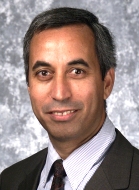
Karl Johnson Ph.D.
Vice President and Senior Fellow
Advanced Packaging Systems Integration Laboratory
Freescale Semiconductor
|
|
| As the semiconductor industry continues in its
pursuit along the curve of Moore’s Law from 65 nm to 45 nm, 32
nm and beyond, the challenges for packaging and assembly
technologies are becoming significant. Packaging can no longer be
thought of as a back end process largely independent of the
silicon and product definition. The assembly and packaging
technologies have become an integral component in the overall
performance, figures of merit and cost competitiveness of these
new generations of products. Further, market trends and customer
expectations are moving rapidly into higher levels of system
integration and system solutions. This trend is moving products
toward greater levels of integration and diversification beyond
the scaling of Moore’s Law.
Rapid market growth in areas beyond the traditional drivers for
the semiconductor industry, such as computer and industrial
applications, into consumer applications with semiconductor based
systems becoming pervasive in all aspects of our lives is placing
additional demands on packaging. These demands include but are not
limited to lower cost, shorter time to market and greater
flexibility and reuse.
This presentation addresses these new challenges, the trends
in packaging and assembly and some unique solutions that are being
developed and implemented. A broad spectrum of products solutions
from system-on-chip, 3D, system-in-package as well as “wafer
level” assembly are discussed.
|
| Dr. Johnson leads the Advanced
Packaging Systems Integration Laboratory (APSL) within the Freescale
Technology Solutions Organization. This laboratory is responsible
for the development and implementation of a broad spectrum of
packaging advances in support of Freescale Semiconductor’s
business and strategy. These innovations are in areas which include
analog power, RF and sensor modules, automotive applications and
advanced wirebond and flip chip packages.
|
|
|
|
Session 1 |
Fine
Pitch PCB Challenges |
2008s1.pdf
(886 KB)
|
| This
opening session explores the challenges faced when dealing with how
high pin count and fine pitch applications impact PCB design and the
assembly and test process. You'll hear about incorporating new
technologies into the socket design to help with PCB assembly issues, a
new interposer option to reduce costs and address typical issues with PCB
assembly and to round out this session, a discussion on diagnosing issues
with high density fine pitch boards. |
|
"Super-Sockets: Integration of Technology
From Test Board Into Socket Assembly" |
Darren Young
Anestal Corporation |
Tom Bresnan
R&D Circuits, Inc. |
|
|
"Column
Failure on Memory Burn-In Boards" |
Yogesh Ahuja
Pycon Inc. |
|
|
|
|
|
|
|
Session 2 |
Clean
Up Your (Socket) Act |
2008s2.pdf
(2.15 MB)
|
| The
papers in this session focuses on cleaning up the down and dirty side
of BiTS applications. The common contamination enemies of production
electrical contacts is examined from a number of different angles. We start with the methods and techniques used in the initial
identification of failed and failing contacts, followed by a post mortem
examination of failed contacts. Finally, various cleaning techniques and
methods used to refurbish / restore contacts are presented. This
session promises to raise your awareness of socket cleaning challenges and
solutions. |
| "An Examination
of the Causes of Cres Degradation Which Affect the Life of
a Test Socket" |
Nick
Langston Jr.
Antares Advanced Test Technologies |
|
| "Improved Method
for Socket Evaluation, Development and Cleaning" |
Terence Q. Collier
CVInc. |
|
|
"CO2
Composite Spray Technology For Test Socket Cleaning"
 |
David Jackson
Cool Clean Technologies |
|
|
"Batting
Cleanup: Approaches to Maintenance of WLCSP Probe Card Interposers"
 |
Jon Diller
Interconnect Devices, Inc. |
Jamie Andes
Interconnect Devices, Inc. |
|
|
|
Session 3 |
Sockets: On the Floor, In
the Lab |
2008s3.pdf
(1.77 MB)
|
| The
application to test devices either in the field or in the lab should
determine the socket or contactor. Once selected, the appropriate usage
envelope, especially under extreme thermal and power conditions, must be
designed and established. And during production testing the necessary
tools must be available to analyze the usage of the sockets to control
performance and cost. All three aspects, selection, usage and field
analysis are addressed during this session. |
| "Contactor
Selection Criteria Overview for RF Component Testing" |
James Migliaccio, Ph. D.
RF Microdevices |
|
|
| "Design
Optimized, Manufacturing Limited - A 250W Thermal Solution" |
Trevor Moody
Antares Advanced Test Tech. |
Kevin Hanson
Antares Advanced Test Tech. |
Rick Davis
Antares Advanced Test Tech. |
| "Test Socket
Tracking: From Cradle to Grave" |
Angelo M. Giaimo
IBM Corporation |
|
|
|
| Poster
Session 1 |
|
2008p1.pdf
(1.03 MB)
|
|
This is the first of two poster sessions. .
|
"Complete Z0
= 50 Ohm Coaxial Spring Probe IC Socket"
 |
Tatsumi Watabe
S.E.R. Corporation |
|
|
| "High Frequency
Wafer Level Test Approach with Coaxial Socket" |
Craig Hudson
Yokowo Co., Ltd. |
Takuto Yoshida
Yokowo Co., Ltd. |
Takahiro Nagata
Yokowo Co., Ltd. |
Atushi Sato
Yokowo Co., Ltd. |
Satoshi Kakegawa
Yokowo
Co., Ltd. |
|
| "Signal and
Power Integrity Analysis of ATE
Loadboard Socket and Package" |
James Zhou
Antares Advanced Test Tech. |
Hongjun Yao
Antares Advanced Test Tech. |
Wei Wang
Sigrity, Inc. |
| "Fine Pitch
Socket Solution" |
Shunji Abe
Yamaichi Electronics Co., Ltd. |
|
|
|
|
|
CHALLENGES
DAY |
|
Session 4 |
Thermal Issues - A Better Understanding |
2008s4.pdf
(1.50 MB) |
| The
Power/Thermal envelope continues to be pushed unremittingly as device
power increases - driving constant investigation into methods and
techniques to come up with the best solution for BiTS applications. To
foster a basic understanding, we kick things off and with a brief
synopsis of thermodynamics principles, thermal modeling and a look at the
entire stack-up of materials and interfaces in the industry today.
Following that, we dig into the critical factors of thermal paths,
interface materials, and heat transfer across different materials. |
"Thermal Design
and Analysis"
 |
Harlan Faller
Johnstech International |
|
|
| "Chasing Die
Temp - What Impacts the Actual Die Temp in Burn-in? How About the
Socket?" |
Mike Noel
Freescale |
Doug Grover
Freescale |
Doug Laing
Freescale |
Dan Wilcox
Freescale |
|
|
| "Metal
Interface Materials for Burn-in Applications" |
Jordan Ross
Indium Corporation |
|
|
"Optimized Air
Cooled Test Socket"
 |
Grant Wagner
IBM Microelectronics |
David Gardell
IBM Microelectronics
|
|
|
|
Session 5 |
Innovative Contact Techniques |
2008s5.pdf
(2.54 MB) |
| It
is a platitude that new package shrinks, and higher frequencies require
new contact technologies. Simply improving certain parameters of a
contactor are not sufficient enough in the long term. Therefore advanced
technologies are required to contact the device or even test without
contacting the device. But the market demands that lower price must go
hand-in-hand with better functionality. In this session, learn about
new contacting concepts and their cost aspects. |
| “Contact Pin
Complexities: Valuing Performance and Cost” |
Paul Schubring
Plastronics |
|
|
“New Concept in
Spring Probe Design”
 |
John Winter
Rika Denshi America, Inc. |
Larre Nelson
Rika Denshi America, Inc. |
Amos Friedner
Rika Denshi America, Inc. |
| “Non-Contact
System-in-Package Testing” |
Jeff Hintzke
Scanimetrics, Inc. |
Chris Sellathamby
Scanimetrics, Inc. |
Brian Moore
Scanimetrics, Inc. |
|
| Hot Topics Session |
From Evaluation to Practice |
2008ht.pdf
(2.13MB) |
| Each
year the Hot Topics Session highlights work that covers one or more
current or emerging high focus themes. Currently among them are three
subjects that are receiving a great deal of attention: contamination,
wafer scale test and advanced modeling and simulation techniques/methods.
In this 4-paper session, each author explores and shares their novel
approach to one of these topics. |
| "Keeping
It Real: Simulating QFN and BGA Probe Performance in the Test Lab" |
Kevin Deford
Synergetix |
Nick Argyros
Synergetix |
Jon Diller
Synergetix |
| "Finite
Element Analysis Using Elastic Membrane Technique for Test Socket
Design Optimization" |
K.
Prabakaran
Antares Advanced Test Tech. |
Ila Pal
Antares Advanced Test Tech. |
|
| "High-Performance
Contactors for Wafer-Level Test (WLT)" |
Jim Brandes
Everett Charles Technologies |
|
|
| "A
Latch System for the Delicate IC Package" |
Hideyuki
Takahashi
Sensata Technologies Inc. |
Hide
Furukawa
Sensata Technologies Inc. |
|
|
| Poster
Session 2 |
|
2008p2.pdf
(2.22 MB) |
|
This is the second of two poster sessions. |
| "Kelvin Contacting" |
Jim Brandes
Everett Charles Technologies |
|
|
| "Use
Simulation to Obtain S Parameters and Network Parameters for
Sockets and PCB/Connectors" |
Sultan Faiz
Ironwood Electronics |
Mike Fedde
Ironwood Electronics |
|
| "New
Solution for Chipscale RF Lead Free ATE Test" |
Sergio Diaz
Ardent Concepts, Inc. |
|
|
| "1mm
Length Spring Probe Practical? - A Study of Spring Pin Dimension
Limit" |
Jiachun
(Frank) Zhou
Antares Advanced Test Tech. |
Praveen
Matlapudi
Antares Advanced Test Tech. |
Mark Murdza
Antares Advanced Test Tech. |
| "Challenges
of Surface Mounted Test Sockets" |
Dr. Shih-Wei
Hsiao
Foxconn |
Andrew
Gattuso
Foxconn |
|
|
|
|
DESIGN
DAY |
|
Session 6 |
Key
Challenges and Technology Trends in Socket Design |
2008s6.pdf
(2.28 MB) |
| Keeping
pace with the Packaging Industry's increasingly complex & ever
demanding requirements for unique applications, higher speeds, and higher
pin counts presents a significant challenge to Test & Burn-in tooling.
With this, the design of effective & reliable socketing solutions
often requires an understanding of the critical design elements
surrounding the interface between the socket and the DUT package, as well
as with the test board. In this session the authors share
assessments, concerns, and various solutions that help improve overall
socket design and performance. |
| "Automated
Topside and Bottomside Testing of POP Packages on a Robotic
Handler" |
Eric Pensa
Texas Instruments |
Willie Jerrels
Texas Instruments
|
|
| "High
Speed Contactor Interconnect" |
David
Mahoney
Xilinx, Inc. |
Hongjun Yao
Antares Advanced Test Tech. |
|
| "Particle
Interconnect: Simple and Effective Socket Solution" |
Robert
Howell
Exatron |
|
|
|
|
|
|
|
|
Session 7 |
High Frequency Developments |
2008s7.pdf
(1.56 MB) |
| High
frequency requirements generate special challenges. In this session
several of these challenges are examined including the impact on the
test environment posed by differential signal technology, and the effect
device placement and alignment accuracy has on RF performance. Rounding
out this session is a discussion of a high speed test interface that
enables up to 400Mhz testing in a highly parallel test system. |
| "Challenging
Device Interface for High Speed DIMM Module Testing" |
| Joachim Moerbt Advantest
(Europe) GmbH |
Rose Hu
Advantest (Europe) GmbH |
|
| "Tolerance
Induced Test Socket RF Performance Variation" |
Gert Hohenwarter
GateWave Northern, Inc. |
|
|
| "From
Single-Ended to Differential" |
Ryan Satrom
Everett Charles Technologies |
|
| Awards
/ Closing Remarks
|
2008closing.pdf
(302 KB) |
|
|
|
|
|
Page last modified
03/28/11
|
 |
BiTS WorkshopTM is a production of
BiTS Workshop LLC |
|