Online October 27 - 29, 2020
Abstract (English)
All the normal indicators we use to determine the health of the semiconductor industry look good. However, two significant and unpredictable factors are in play: COVID-19 and the US-China trade dispute. Clearly, these are not normal times, which means we should be looking at alternative data sets to help guide our decision making. This presentation reviews the industry's current state and explains what other types of information we can use to give an early warning of any shift in market conditions.
摘要 (Chinese)
虽然我们用来确定半导体行业健康状况的各项指标看起来都不错。但是有两个重要且不可预测的因素正在起作用:新冠病毒和中美贸易争端。显然,这是特殊情况,意味着我们应该研究下备选项数据信息以辅助我们决策。本演讲回顾了半导体行业的现状,并说明了我们可以使用哪些其他类型信息来对市场状况的任何变化做出预警。
 Managing Director
“5G毫米波设备的射频测试策略和解决方案”
Abstract - Biography (English)
As 5G products begin production ramp several new test challenges are being addressed by test equipment providers. For 5G millimeter wave products, over-the-air radiated tests present a new set of test challenges as compared to sub-6 GHz products. This presentation provides and overview of the new test challenges for 5G devices and test solutions by Teradyne, including capability for testing millimeter wave devices, easy ATE upgrade path from traditional sub-6GHz to millimeter wave testing, higher port-count instrumentation for testing high-density millimeter wave phase array antennas elements, over-the-air test techniques for module-level devices and others.
Jeorge S. Hurtarte is currently Wireless Product Marketing Strategist at Teradyne, Boston, USA. Mr. Hurtarte has held various technical and management positions at Teradyne, LitePoint, TranSwitch, and Rockwell Semiconductors. He holds Ph.D. and B.S. degrees in electrical engineering, an M.S. in telecommunications, and an M.B.A. Mr. Hurtarte has served on the Advisory Board of Directors of the Global Semiconductor Alliance, TUV Rheinland of North America, and the NSF’s Wireless Internet Center for Advanced RF Technology. He is the secretary of the IEEE 802.11ay task group. Dr Hurtarte is also professor at the University of California, Santa Cruz and at the University of Phoenix, Bay Area, California. He is also the lead co-author of the book Understanding Fabless IC Technology.
摘要 - 简介 (Chinese)
随着5G产品开始量产,测试设备提供商正在应对一些新的测试挑战。对于5G毫米波产品,与6 GHz以下的产品相比,空中辐射测试提出了一系列新的测试挑战。本演示文稿概述了Teradyne针对5G设备和测试解决方案所面临的新测试挑战,包括测试毫米波设备的能力,从传统的6GHz以下到毫米波测试的轻松ATE升级路径,用于测试高带宽的更高端口数的仪器密度毫米波相控阵天线元件,用于模块级设备的空中测试技术等。
Jeorge S. Hurtarte目前是美国波士顿Teradyne的无线产品营销策略师。 Hurtarte先生曾在Teradyne,LitePoint,TranSwitch和Rockwell Semiconductors担任过各种技术和管理职务。他拥有博士学位。和B.S.电气工程学士学. Hurtarte先生曾在电信领域任职,并曾担任全球半导体联盟,北美TUV Rheinland和NSF的高级射频技术无线互联网中心的顾问委员会成员。他是IEEE 802.11ay任务组的秘书。Hurtarte博士还是加利福尼亚大学圣克鲁斯分校和加利福尼亚湾区凤凰城大学的教授。他还是《了解无晶圆厂集成电路技术》一书的主要合著者。
“晶圆级MEMS测试”
Abstract - Biography (English)
Currently almost all final test is done in stimulus test systems with pick and place handling, because this is needed when sensors are packaged in traditional packages. Applying these pick and place solutions to small CSP packages with sizes of 1x1mm or even smaller introduces challenges that can be avoided when final test is moved to a wafer probe station that allows testing under stimulus.
Our talk explores the advantages of wafer level test in regards to device performance and benefits for manufacturing at the test floor.
Michael has more than 25 years of experience in the semiconductor industry and is currently holding a position as Director Sales and Marketing with Afore Oy, a Finland based provider of application specific test solutions for MEMS and other semiconductor devices. In this position he has high visibility on current and future requirements for test applications, especially in regards to final test and calibration of MEMS sensors. Michael has a technical background and started his career as service and applications engineer for laser based marking and process equipment supporting first a European and then a global customer base. Prior to his appointment with Afore he held several sales and marketing positions for semiconductor equipment related to wafer metrology, device handling and reliability.
摘要 - 简介 (Chinese)
当前,几乎所有的最终测试都是在带有拾取和放置处理功能的刺激测试系统中完成的,因为当传感器以传统包装方式包装时,这是必需的。 将这些拾取和放置解决方案应用于尺寸为1x1mm或更小的小型CSP封装带来了挑战,当最终测试移至允许在激励下进行测试的晶圆探针台时,可以避免这些挑战。
我们的演讲探讨了晶圆级测试在设备性能方面的优势以及在测试平台上制造的益处
Michael在半导体行业拥有超过25年的经验,目前担任Afore-Oy的销售和市场总监,Afore- Oy是芬兰的MEMS和其他半导体器件专用测试解决方案提供商。在此职位上,他对测试应用程序的当前和未来要求具有很高的知名度,尤其是在MEMS传感器的最终测试和校准方面。 Michael拥有技术背景,并从服务和应用工程师开始其职业生涯,主要是为激光打标和处理设备服务,首先为欧洲客户,然后为全球客户提供支持。在被任命为Afore之前,他曾担任过与晶圆计量,设备处理和可靠性相关的半导体设备销售和营销职位。
“内部和外部的变化驱使半导体测试行业适应新现实”
Abstract - Biography (English)
Whatever happens next, 2020 will be the year when the industry was forced to change, and change quickly, to the new reality. Factors outside our control: COVID-19 and the US-China trade dispute will permanently change the way of human life and roll back the globalization of commerce.
These changes, in turn, are forcing companies to rethink their strategies and priorities so that they can make the right decisions going forward about the internal factors they can control.
This presentation explores the impact of COVID-19 and the US-China trade dispute on the semiconductor industry and what this means for semiconductor test. In particular, how supply chains are reconfiguring, how the end-users such as Apple, Google, Facebook, etc., are becoming more influential, and how test strategies are evolving in response.
To help you successfully navigate these changes, we will review some of the data and information you will need to make the right decisions.
Lin is a Technical and Market Analyst of VLSI Research Europe. She received the bachelor’s degree in electrical engineering from Edinburgh University in 2013. Then, she started her postgraduate study in Cambridge University. In the meantime, she published more than ten papers as the first author or co-author in the IEEE Transactions. In 2017, she received the Doctoral Degree in Engineering from Cambridge University and started to work in VLSI Research Europe. At present, she focuses on the marketing research and analysis related to semiconductor test consumables.
摘要 - 简介 (Chinese)
内部和外部的变化驱使半导体测试行业适应新现实 无论接下来发生什么,2020年将是半导体行业为适应新现实被迫改变,并迅速改变的一年。我 们无法控制的因素包括:COVID-19和中美贸易争端将永久改变人类的生活方式,并阻碍商业全 球化。 这些变化也正在迫使公司重新考虑其相关战略和优先次序,以便他们能够就自己可控的内部因 素做出正确的决策。 此次演讲将探讨COVID-19和中美贸易争端对半导体行业的影响以及这对半导体测试领域的意义 。特别是,供应链如何进行重新配置,苹果,谷歌,脸书等终端用户如何变得更有影响力,以 及测试策略如何相应地发展。 为了帮助您成功应对这些改变并做出正确决策,我们将提供所需的一些市场数据和信息。
付琳于2013年毕业于爱丁堡大学,并获得电气工程一等荣誉学士学位。同年,在剑桥大学 继续研究生学习。期间,她作为第一作者或合作者在国际期刊及会议上发表论文十余篇 。2017年,付琳取得剑桥大学工学博士学位并开始在VLSI Research Europe工作。目前, 她致力于半导体测试领域的市场研究与分析。
“最低安培成本的模块化和高保真宽带DPS”
Abstract - Biography (English)
“The wide spectrum of SOC and SiP devices are driving a large range of DUT power supply requirements. Power supply requirements range from low power 1 Watt per device with up to 5 different voltages to high end GPU/Processors with switching requirements from 10 Watts to more than 150 Watts within a few microseconds.
Users can address the low power requirement with ‘off the shelve’ instruments and most ATE systems. However, the high-power coverage is still limited to a small number of high end solutions manufacturers.
Considering that only dedicated amplifiers can cover the need for high power devices, the traditional answer it to populate scarce and expensive ATE slots with a suite of high-power Device Power Supply’s.
Mu-Test, an AEM company, is addressing these challenges by developing a unique Power supply module that covers low power/high accuracy and High power device needs while maintaining the required signal fidelity at an affordable cost.
This paper will share the requirements, technical challenges, solutions and supporting data to address these demanding device power supply challenges.”
Mathieu Duprez has more than 30 years of experience in R&D in ATE and measurement industry. Graduated with Master’s degree in Electronic and semiconductor physics, he spent the first 20 years of his career within Schlumberger/NPTest/Credence design groups. As design engineer and project manager, he has been conceiving state of the art instruments and system architectures from DC to multi Gbps.
He founded Mu-test in 2008, providing semi conductor industry with a major cost breakdown and the comprehensive, scalable test platform required by SOC devices and upcoming technologies.
Since 2020, he is heading AEM’s ATE core technology team in France and Singapore
摘要 - 简介 (Chinese)
各种各样的SOC和SiP器件正在推动各种DUT电源需求。电源要求的范围从每设备最多5种不同电压的1瓦低功耗到在几微秒内从10瓦到150瓦以上的开关要求的高端GPU /处理器。
用户可以使用“货架”仪器和大多数ATE系统来满足低功耗要求。但是,高功率覆盖范围仍然仅限于少数高端解决方案制造商
考虑到只有专用放大器才能满足大功率设备的需求,传统的解决方案是使用一套大功率设备电源来填充稀缺且昂贵的ATE插槽。
AEM公司Mu-Test通过开发独特的电源模块来应对这些挑战,该模块可满足低功率/高精度和高功率设备的需求,同时以合理的成本保持所需的信号保真度。
本文将共享要求,技术挑战,解决方案和支持数据,以解决这些苛刻的设备电源挑战。
马修·杜普雷斯(Mathieu Duprez)
马修·杜普雷斯在ATE和测量行业的研发中拥有30多年的经验。 毕业后,拥有电子和半导体物理学硕士学位的他,首20年在Schlumberger / NPTest / Credence设计团队工作。 当时作为设计工程师和项目经理,他一直在构想为DC, multi- Gbps等,开发更先进的仪器和系统架构。
他于2008年创立了Mu-test,为半导体行业提供主要的成本细分以及SOC设备和即将推出的 技术所需的全面,可扩展的测试平台。
自2020年,他被任命主导法国和新加坡AEM ATE的核心技术团队 。
“AI和高性能处理器的高功率测试挑战”

Abstract - Biography (English)
Advanced process large-scale chip products such as AI applications are constantly driving the power output capabilities of test platforms. Many products for the server high-performance computing market have power consumption as high as 400w. In ATE (Automatic Testing Equipment) mass production testing, the higher Toggle rate will even reach several times the peak power consumption. The constantly evolving test trend also requires that test solutions need to increase test parallelism as much as possible, increase support for more power rails and parallelism, and thus reduce processing costs. In addition, the lower and lower core voltage also puts higher and higher requirements on the output accuracy and dynamic response of the power supply.
This presentation will discuss the power supply challenges encountered by current high-performance processors and AI products, and how to deal with these challenges in terms of mass production. It will analyze and interpret different power supply test challenges for several different test scenarios: high density and high parallelism, high current and low voltage, and high dynamic response performance.
Beck Yu is positioned as Field Product specialist at Teradyne China Sales team, focus on fields like Digital, RF, Power, Mixed signal semiconductor testing solution design & development and product marketing support.
摘要 - 简介 (Chinese)
AI及高性能处理器的大功率测试挑战 / High-power test challenges for AI and high-performance processors 先进制程的大规模芯片产品如AI应用,正在不断驱动着测试平台的功率输出能力。很多针对服务器高性能运算市场的产品,其功耗已经高至400w,在ATE(Automatic Testing Equipment)量产测试中较高的Toggle rate甚至会达到数倍的峰值功耗。不断演进的测试趋势也要求测试方案需尽可能提高测试并行度,增大对更多电源轨以及并行度的支持,从而降低加工成本。另外越来越低的核心电压也对电源的输出精度,以及动态响应提出了越来越高的要求。
本文会针对当下高性能处理器及AI产品遇到的供电挑战,以及如何在大规模量产角度应对这些挑战进行详细讨论。会针对几种不同测试场景:高密度高并行度,大电流低电压,以及高动态响应性能的不同电源测试挑战案例进行分析解读。
于波是负责泰瑞达中国区销售团队的市场专家,专注于数字,射频,功率,混合信号半导体产品的测试方案定制 以及 对应市场产品的开发决策支持。
“在可测性,功能安全性和安全性方面满足未来的可靠性半导体需求”
Abstract - Biography (English)
Meeting the Reliability Semiconductor needs of the future in the Testability, Functional Safety and Security We stress the importance of a platform that allows a continuous monitoring of the most significant reliability parameters and to be able to build a database of these measures from which learn about failures and trigger continues improvement of product and process. Finally, we outline a potential solution to the semiconductor field aimed at releasing the testing approach from the software to a specific proprietary hardware proposing an integrated design, simulation and debugging environment (called Meta IDE). This independent software platform creates an automated seamless flow from design to testing using the methodology indicated, along with a universal translation/conversion to any kind of target testing machine. In this way the user, thanks to this independent software platform, will be free to use any type of testing equipment.
Luca Moriconi holds a degree in Electronic Engineering from the University Of Perugia, Italy. He joined ELES Semiconductor Equipment - Italy - in1999 and worked for16 years in the semiconductor reliability and testing industry as Senior Application Engineer and then Test Application Division Manager.
Luca is currently Solution Roadmap Manager at ELES and works to define and deploy the technical roadmap of the ELES solutions.
摘要 - 简介 (Chinese)
我们强调平台的重要性,该平台可以连续监视最重要的可靠性参数,并能够建立这些措施的数据库,从而从中了解故障并触发产品和过程的持续改进。 最后,我们概述了半导体领域的潜在解决方案,旨在将测试方法从软件发布到特定的专有硬件,从而提出集成设计,仿真和调试环境(称为Meta IDE)。 这个独立的软件平台使用指定的方法创建了从设计到测试的自动化无缝流程,并且可以通用转换/转换为任何类型的目标测试机。 这样,由于有了这个独立的软件平台,用户将可以自由使用任何类型的测试设备。
Luca Moriconi拥有意大利佩鲁贾大学的电子工程学位。 他于1999年加入意大利ELES半导体设备公司,在半导体可靠性领域工作了16年。 和测试行业的高级应用工程师,然后是测试应用部门经理。
Luca目前是ELES解决方案路线图经理,致力于定义和部署ELES解决方案的技术路线图。
“Sub-6G功率放大器的ATE測試挑戰”
Abstract - Biography (English)
Sub-6G RF TRX system is hot spot in 5G communication. Compared to mm-wave band (FR2), sub-6G (FR1) band has a lower power consumption and larger cover range. Compared to traditional 3G/4G Front End Module (FEM), sub-6G FEM also brings challenges like obvious occupied band-width increase (10M/20MHz-> 100/200MHz), higher order modulation (64QAM -> 256QAM). At the same time, the efficiency of Sub6G Power Amplifier (PA) is reduced fiercely. The biggest question we faced in the Sub6G PA is the thermal degradation caused by extremely low power added efficiency (PAE) in ATE test condition.
Our ATE test environment were established on the latest Advantest SmarTest8 (SW) and V93K tester (HW). Compared to customer’s environment, ATE test environment works with higher density (WSRF card), shorter time, worse heat dissipation, multiple RF connectors and attenuators. Worse heat dissipation means EVB-IC is welded to EVB PCB, larger contacting GND(6-Pads) exists on EVB while ATE use two socket pogo as GND. PA active current was over than 1A at an output power 26.5dBm without no additional heat dissipation method. Shorter time: customer-RD does not care about the test time in their side, what they want just accuracy results, while ATE cares much about the test time.
Critical ATE test environment and tight schedule, but we still need to ensure correct test results, a careful correlation scheme is essential and been well designed. This article explains how to overcome the non-convergence of the reference calibration current, how to reproduce the results of calibration and FT, and how to ensure the robustness of the results of mass production testing from the perspective of engineering and production. We hope this article will be helpful to the other similar ICs engineering practice and rapid introduction.
Norris Wang, born in 1989,12. Graduated from Tongji University in 2015 with a master's degree in Physics and Science. 2015-2019, RF application engineer (ZTE/Thundersoft). 2019-3, joined Advantest Shanghai as ATE engineer.
摘要 (Chinese)
最近两年来,Sub-6G射频TRX系统是5G通信。与毫米波段(FR2)相比,亚6G波段(FR1)具有更低的功耗和更大的覆盖范围。与传统的3G/4G前端模块(FEM)相比,sub-6G前端模块也带来了占用带宽明显增加(10M/20MHz->100/200MHz)、高阶调制(64QAM->256QAM)等挑战。同时,Sub6G功率放大器(PA)的效率急剧下降。Sub6G功率放大器面临的最大问题是ATE测试条件下极低的功率附加效率(PAE)引起的热退化。
我们的ATE测试环境建立在最新的Advantest SmarTest8(软件)和V93K测试机台(HW)上。与客户环境相比,ATE测试环境具有更高的密度(WSRF板卡4site同测)、更短的时间、更差的散热(几乎没有)、多个射频连接器和衰减器。散热差意味着EVB-IC焊接在EVB-PCB上,EVB上存在较大的接触GND(6-Pads),而ATE使用两个插座pogo作为GND,在我们遇到的实际案例中,在没有附加散热措施的情况下,DUT输出功率为26.5dBm时,DUT工作电流大于1A。ATE永远面临着尽可能减少时间的问题,而客户的研发并不关心他们的测试时间,他们想要的只是准确的结果,这也给我们做数据对齐带来了很大的挑战。
极端的ATE测试环境和紧张的时间表,我们仍然需要确保正确的测试结果,一个仔细的相关方案是必不可少的。本文从工程和量产的角度出发,阐述了如何克服基准校准电流的不收敛性,如何再现标定和FT的结果,以及如何保证量产试验结果的稳健性。希望本文能对其他类似的集成电路工程实践和快速介绍有所帮助。
“高速測試插座之射頻仿真技術”
Abstract - Biography (English)
The rise of Internet of Things, 5G, artificial intelligence, autonomous cars, Deep Learning, self-driving vehicles have increased consumer demand for products requiring higher speed digital and analog Integrated Circuits (ICs), therefore, the demand for designing high performance test sockets must keep pace.
In this paper, we will discuss the challenge of RF simulation and will focus on a new Enhanced Simulation Technique that can improve the accuracy of simulation, validation methods with advanced measurement to show correlation study between simulation and actual measurement
In Signal Integrity simulation, HFSS software is commonly used especially for high frequency. As Data rates and Bandwidth continue to increase, a paradigm shift is emerging in the industry which is driving socket suppliers to provide more detailed simulations to include the Device Package and PCB interfaces in the analysis. It is critical that the socket impedance is matched as closely to the PCB impedance for maximum performance.
VNA measurement verification. A Vector Network Analyzer play a key role to achieve correlation between simulations and measurement, The VNA measures the amount of energy transmitted through the DUT and reflected by the DUT at different frequencies. It then provides these results in scattering-parameter (S-parameter) of the entire test setup. The test socket is then de-embedded and gated to try and provide basic performance data, such as the -1 dB Insertion Loss (IL), -10 dB Return Loss (RL), Loop Inductance (L), Mutual Capacitance (Cm) IL, without the effects of test fixtures and PCB.
In conclusion, SI simulations using HFSS become critical in developing new high-speed test sockets. Extensive simulation can reduce development time. More importantly, optimized simulation methodology by including package and test board structures can generate more accurate or reliable simulation results.
Khaled Elmadbouly is a Signal Integrity Design Engineer with Smiths Interconnect. He has twenty-five years of experience in semiconductor front and backend testing process include PCB design, high speed device contactor, and HFSS Signal Integrity simulation. He earned a BSEE degree from San Jose State University and a BS Mathematical Statistics from Cairo University.
摘要 - 简介 (Chinese)
隨著物聯網,5G,人工智能,自動駕駛汽車,深度學習,自動駕駛汽車的興起使消費者對需要更高速度的數字和模擬集成電路(IC)的產品的需求增加,因此,對設計高性能測試插座的需求也不斷增加必須保持同步。
在本文中,我們將討論射頻仿真的挑戰,並將重點介紹一種新的增強型仿真技術,該技術可以提高仿真的準確性,並通過先進的測量方法來驗證方法,以顯示仿真與實際測量之間的相關性研究。
在信號完整性仿真中,HFSS軟件通常用於高頻。隨著數據速率和帶寬的不斷提高,業界正在出現一種範式轉移,這促使插座供應商提供更詳細的仿真,以將設備封裝和PCB接口涵蓋在分析中。至關重要的是,插座阻抗必須與PCB阻抗緊密匹配,以實現最佳性能。
VNA測量驗證。矢量網絡分析儀在實現仿真與測量之間的相關性方面起著關鍵作用。VNA測量通過DUT傳輸並在不同頻率下被DUT反射的能量。然後,在整個測試設置的散射參數(S參數)中提供這些結果。然後,將測試插座去嵌入和選通,以嘗試提供基本的性能數據,例如-1 dB插入損耗(IL),-10 dB回波損耗(RL),環路電感(L),互電容(Cm) IL,不受測試夾具和PCB的影響。
總之,使用HFSS進行SI模擬對於開發新的高速測試插座至關重要。廣泛的仿真可以減少開發時間。更重要的是,通過包括封裝和測試板結構的優化仿真方法可以生成更準確或更可靠的仿真結果。
Khaled Elmadbouly是Smiths Interconnect的SI設計工程師(信號完整性)。 他在半導體前端和後端測試過程中有25年的經驗,包括PCB設計,高速晶片插座和HFSS信號完整性仿真。 他取得了San Jose州立大學的電機工程學士學位和Cairo大學的數學統計學士學位。
“超越回环法的高速串行测试”
Abstract - Biography (English)
Traditionally, serial I/O ports have been tested using loopback methods, where the transmit port is connected to the receive port and internal BIST algorithms are used by the device to test itself. With the newest generations of high-speed port testing including 56Gbd PAM4, devices need to be better characterized to prepare them for a more challenging environment. Rather than loopback alone, external sampling scopes and BERTs can be used to test these devices more thoroughly with additional data collection that offers potential for better device margining, more thorough data sheet specification checking and troubleshooting beyond pass/fail testing. MultiLane will present data to compare a device tested by loopback-only versus the same device tested using a MultiLane BERT and Scope to show the benefits of breaking with the paradigm of loopback-only testing.
An Advantest V93000 including a Multilane high-speed option will be used to do the comparison. A loadboard was designed to simultaneously test two of the same high-speed devices; one device using traditional loopback and one device using Multilane scopes and BERTs to do more complete testing. This real data will be shared in the presentation and pertinent simulation data will also be shared. The presentation will also go into the mechanics of connecting the scopes and BERTs to the loadboard and into how to de-embed the 56Gbd PAM4 signals.
Doug Malech has 30 years in various engineering design, sales and marketing roles in both ATE and semiconductor companies.
摘要 - 简介 (Chinese)
传统上,串行I / O端口是使用回环方法进行测试的,其中发送端口连接到接收端口,并且设备使用内部BIST算法对其自身进行测试。随着包括56Gbd PAM4在内的最新一代高速端口测试的出现,需要对设备进行更好的性能表征,以便为更具挑战性的环境做好准备。不仅可以单独使用环回,还可以使用外部采样示波器和BERT通过附加数据收集来更彻底地测试这些设备,这些数据可以提供更好的设备保证金,更彻底的数据手册规格检查以及通过/失败测试之外的故障排除。 MultiLane将提供数据,以比较仅环回测试的设备与使用MultiLane BERT和Scope测试的同一设备,以展示突破仅环回测试范式的好处。
比较将使用包含Multilane高速选件的Advantest V93000。负载板旨在同时测试两个相同的高速设备。一台使用传统环回的设备,另一台使用Multilane示波器和BERT的设备进行更全面的测试。此真实数据将在演示中共享,并且相关的模拟数据也将共享。该演讲还将探讨将示波器和BERT连接到负载板上的机制,以及如何去嵌入56Gbd PAM4信号。
ATE和半导体公司中担任30年的设计,销售和营销职务. 现在,是销售经理
“下一世代之測試單元與測試操作”
Abstract - Biography (English)
Requirement to perform bench testing is getting more and more challenging due to complexity of system/board integration design. Example: measuring multiple voltage signal from a single reference validation board by using ordinary 4 channel of oscilloscope. The situation could be even more challenging if an engineer needs to perform power sequencing test by using ordinary 4 channel oscilloscope. Intel has come out with a breakthrough solution to simulate the physical oscilloscope function with a FPGA solution, improve the overall test time and automate the reporting work. This solution also enables remote probing capability and enable cloud based remote debug in Intel.
Intel is using this invention to support the next generation of product design and successfully proof a total of 50% (approximately) reduction in oscilloscope purchase and improve 99% efficiency in bench testing which dealing with signal measurement. This solution also helps to enable cloud based remote debug infrastructure in Intel.
See Tien "Angie" Ng graduated with Master in Engineering (major in microelectronics) from Multimedia University Malaysia. She currently pursuing a part time doctorate study with University Science Malaysia. Angie is Technical Lead for Intel Malaysia Internet of Things Group, a certified FUSA Automotive Engineer with 23 years of industrial working experience.
摘要 - 简介 (Chinese)
由於系統/電路板集成設計的複雜性,執行工程測試的要求變得越來越具有挑戰性。範例:使用示 波器的普通4通道測量來自單個參考驗證板的多個電壓信號。如果工程師需要使用普通的4通道示 波器執行電源時序測試,則情況可能更具挑戰性。英特爾推出了一項突破性的解決方案,可以使 用FPGA解決方案模擬物理示波器功能,縮短總體測試時間並使報告工作自動化。該解決方案還啟 用了遠程探測功能,並在Intel中啟用了基於雲端的遠程除錯。
解決方案實施:英特爾正在使用本發明來支持下一代產品設計,並成功證明了示波器採購量總共 減少了(大約)50%(大約),並在處理信號測量的台式測試中提高了99%的效率。 該解決方案 還有助於在Intel中啟用基於雲的遠程除錯基礎結構。
Angie毕业于馬来西亚的Multimedia University, 微电子专业硕士。目前在University Science Malaysia 攻读博士学位。Angie 是Intel Malaysia IoT 部门的技术领导,拥有FUSA注册工程师, 和23年企业工作经验。
Program subject to change without notice
Event registration is free courtesy of our sponsors
Premier Sponsor
Being in the business since 1979, TTS Group dedicates itself to bringing the best possible solutions to help our customers solve some of the most challenging issues in semiconductor test and tooling today. Right from R&D to design to simulation to validation, we focus on lowering the total cost of final test through relentless pursuit of innovation, yield, quality, reliability and on-time delivery for our customers. We understand our customer needs and provide a one-stop solution for all their concerns.

Honored Sponsor

JDT Technology's focus in the vertical field of semiconductor and electronic product testing & precision manufacturing, and dedicate ourselves to be an “Intelligent Automation Integrated Solution Provider”. Our main business includes: Probe materials, ICT / FCT test fixtures, Automated Testing Equipment & Precision Machining.
Distinguished Sponsors
Nidec SV TCL is a global provider of high-quality semiconductor testing solutions. Our extensive product line includes innovative MEMS Probes and a variety of Probe Card technologies. Our proprietary MEMS Probes are fully customizable, capable of both wafer/final test, and can be utilized for many advanced devices including RF, 5G, Mobile, Auto & IoT. We also have analytical and simulation capabilities along with full turnkey services for probe cards and final test.
Our unmatched worldwide infrastructure provides coverage for major semiconductor regions around the world with full design & manufacturing capabilities for our probe technologies in China, USA, Taiwan, Japan, Korea & Singapore.
Contact us at sales@nidecsvtcl.com to learn more!
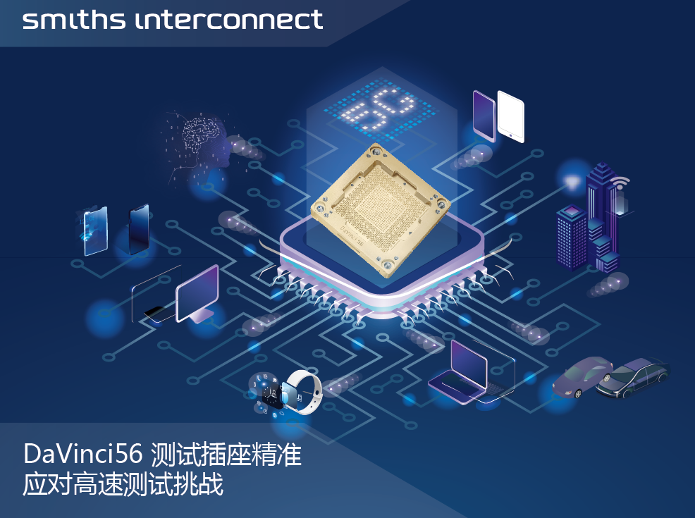
Smiths Interconnect is a leading provider of innovative solutions for critical semiconductor test applications. Smiths Interconnect’s test sockets and probe card solutions offer superior quality and reliability, providing customers with a competitive advantage. Our best-in-class engineering, development and technical expertise ensure support of automated, system level and development test platforms for area array, peripheral, wafer level and Package on Package (PoP) devices as well as high performance spring probe technology and cable assemblies. Our extensive product portfolio accommodates devices with finest micro pitches as well as those with very high bandwidth requirements. Off-the -shelf and custom products are proven to deliver the best solution for the customer’s specific needs.
For more information, please visit www.smithsinterconnect.cn

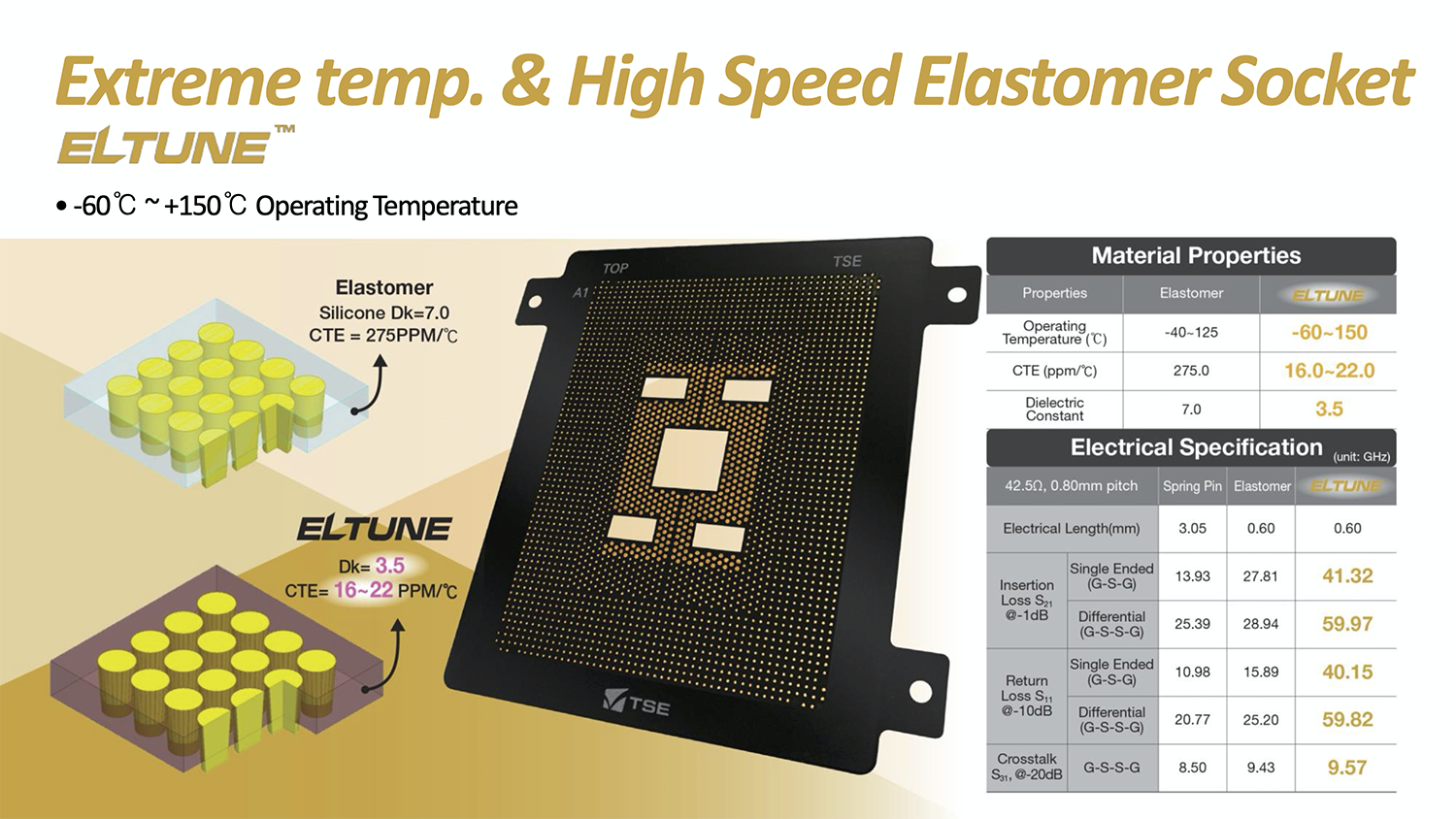
We have been providing test-related products and services to improve the quality and reliability of semiconductors and OLED around the world since TSE Co., LTD. was founded in 1994. Since 2007, TSE has operated its own MEMS Fab to develop and produce MEMS products such as customized particles & contacts, probe pins, inductors, relays, ceramic substrates, etc. The capability to manufacture innovative components in-house enables us to deliver products faster and at lower costs. Our continuous investment and development for products enable us to provide a leading-edge probe card, test interface board, and test socket for semiconductor test.