BiTS is the world's premier workshop dedicated
to providing a forum for the latest information
about burn-in and test tooling, and related
fields. At BiTS you'll find a comprehensive
technical program, exhibits of the latest
products and services, and many opportunities to
meet, network and explore ideas with other test
and burn-in strategies professionals.
Click here if you need the latest Acrobat(R) reader
from Adobe(R):
or
for an alternate free PDF
viewer, download the latest
Sumatra PDF
It is FAST!
BiTS
2013 ARCHIVE PAGE
COPYRIGHT NOTICE
The
paper(s) in this publication comprise
the Proceedings of the 2013 BiTS
Workshop. The content reflects the
opinion of the authors and their
respective companies. They are
reproduced here as they were presented
at the 2013 BiTS Workshop. This version
of the papers may differ from the
version that was distributed in hardcopy
& softcopy form at the 2013 BiTS
Workshop. The inclusion of the papers in
this publication does n ot constitute an
endorsement by BiTS Workshop, LLC or the
workshop’ sponsors. There is NO
copyright protection claimed on the
presentation content by BiTS Workshop,
LLC. (Occasionally a Tutorial and/or
TechTalk may be copyrighted by the
author). However, each presentation is
the work of the authors and their
respective companies: as such, it is
strongly encouraged that any use reflect
proper acknowledgement to the
appropriate source. Any questions
regarding the use of any materials
presented should be directed to the
author(s) or their companies. All photographs on this page are copyrighted by BiTS Workshop LLC. The BiTS logo
and ‘Burn-in & Test Strategies Workshop are trademarks of BiTS Workshop LLC.
All rights reserved.
BiTS 2013 archive access requires
registration. To avoid yet another
username and password, registration is
through your LinkedIn account. Register
as a FREE guest, Full Conference
Attendee (BiTS 2013), or a Subscriber.
Traditional archive content is available
to Guests; Premium content is available
to Attendees and Subscribers.
(Registration Required)
Technical Program
Once again,
the BiTS Workshop offered a robust and riveting program featuring 30+
papers presented during 7 podium and one poster session covering a host
of test and burn-in related topics from a worldwide representation of
authors.
A TechTalk session
started the workshop off by Delta
Design's Jerry Tustaniwskyj, Ph.D., talking
tech about test handlers, addressing a
number of challenges related to testing
today’s high-performance IC devices such
as multi-chip modules, 3-D packages, and
lapped silicon with thinned substrates.
With "Thermal and Mechanical
Challenges for Test Handlers", he zeroed in on thermal control of the DUT, the need for robust pick-and-place
systems, and the importance of vision
systems. Additionally, there was a
brief discussion on requirements for
testing MEMS devices, where in addition
to electrical test, physical excitation
of the device is required.
BiTS got 'down and dirty' with Jerry Broz, Ph.D. of
International Test Solutions, as he
shared his strategies for socket
cleaning, thereby reducing the cost of
test and improving equipment
effectiveness in his
Tutorial
titled, “Package Test is a Dirty
Business !!!”. In this broad tutorial,
Broz discussed various off-line and
on-line socket cleaning practices,
including high volume testing challenges
and solutions for on-line cleaning to
maintain high yield and throughput,
reduce socket repairs, and control
contactor damage.
Talking Points -
Interconnectology New this
year, BiTS Workshop, 3D InCites, and
Impress Labs co-promoted an afternoon
talkshow "hosted" by the Queen of 3D, Françoise von Trapp. The topic was
"Interconnectology: Inspiring a Paradigm
Shift". A move to better define the
next-generation of IC device
manufacturing has led to the emergence
of new terminology focused on the
interconnect vs. the packaging. As such, Interconnectologists specializing in
Interconnectology will try to carve a new space
in the industry.
Keynote
Speaker Bill McClean of IC Insights
addressed "The Dramatic Restructuring of
the Integrated Circuit Industry". In IC
Insights’ opinion, the “bottom” of the
current cycle in the worldwide economy
and IC industry was reached in 2012 and
2013 will mark the beginning of the next
cyclical upturn—one in which the IC
industry CAGR will more than triple to
7.4% in the next 5-year period.
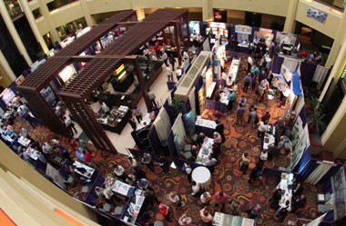
51 exhibitors, from socketing and related industries, exhibited their products and services
during breaks in the technical program. Click
HERE for the exhibitor list of BiTS EXPO 2013.
Participants
BiTS 2013 brought together well over 300 participants,
including nearly 250 full conference attendees, and 51 exhibitors from
around the world, representing end users and suppliers of sockets, boards,
burn-in systems, handlers, packages and other related equipment, materials and
services.
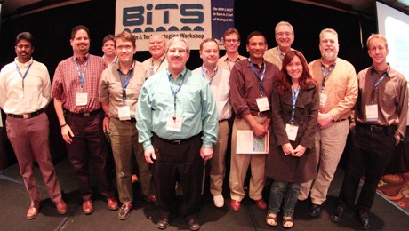
Front:
Ila Pal (Ironwood Electronics), Ira Feldman
(Feldman Engineering), Owen Prillaman (Tech-Connect Sales), Valts
Treibergs (Multitest), Paul Boyce (Advantage Specialist), John Hartstein
(Sensata), Mike Noel (Freescale), Joachim Moerbt (Advantest
Europe),
Rafiq Hussain (AMD), Fred Taber (BiTS
Workshop), CY Lai (Test Tooling Solutions), John Moore (Texas Instruments)
, Morton Jensen (Intel)
Not pictured:
Marc Knox (IBM)
TUTORIAL
DAY
Sunday, March 3, 2013
TechTalk
Thermal and Mechanical Challenges for Test Handlers
Jerry Tustaniwskyj, Ph.D.
Director of Technology Development Delta Design, Inc.
Jerry Tustaniwskyj, Ph.D. earned a Bachelor
of Science and a Ph.D. in Mechanical Engineering from Wayne State
University. He has been the Director of Technology Development at Delta
Design, Inc. since 2006. From 1973 through 2006 he held a range of
positions from engineering intern to Unisys Fellow, involved with
mechanism design, controls, thermal systems, device packaging, at
Burroughs/Unisys. His academic experience includes serving as an
Assistant Professor of Mechanical Engineering at Wayne State University
from 1975 – 1976 and from 1986 to the present as a part time faculty
member in Mechanical and Aerospace Engineering (MAE) at the University
of California, San Diego. Dr. Tustaniwskyj has 47 issued patents, 3
patent applications pending and 16 technical publications. From 2004 to
the present he has served as an evaluator (representing ASME) of
university mechanical engineering programs for ABET (Accreditation Board
for Engineering and Technology).
(Registration Required)
IC devices continue to evolve with higher
functionality and lower cost. This higher functionality means that the device
circuit density is increased as is the corresponding number of IO’s. The overall
size of these devices is decreasing in order to improve performance and be
useable in applications with minimal space such as mobile phones or tablets.
These devices include multi-chip modules, 3-D packages, lapped silicon with
thinned substrates, etc. In order to continue to drive device costs lower, these
more complex devices cannot increase test time, resulting in a real push to
increase the parallelism of test. Unique new challenges exist for test handlers
with these devices during functional test as well as for other test processes
such as burn-in or system level test.
This seminar
addressed a number of challenges related to testing these devices. These
challenges include purely mechanical issues as well thermal. We discuss the need
for more robust pick and place processes along with the precision alignment of
the device under test (DUT) to the contact pins. The use and advances of vision
systems are described. Their benefit is not only in device alignment, but also
for process control and diagnostics. We review the material property and thermal
expansion issues related to testing at extreme temperatures (tri-temp).
A considerable portion of the seminar was dedicated to thermal
control of the DUT. Traditional methods need to be modified in order to control
device temperature with the new packaging technologies. Discussed were the thermal
challenges of designing highly parallel passive systems along with active
thermal control for each DUT. Cost versus performance tradeoffs are addressed
for both low and high power dissipating devices as well as the pros and cons of
air, liquid, phase change, and thermoelectric cooling systems.
Included is a brief discussion on requirements for
testing MEMS devices, where in addition to electrical test, physical excitation
of the device is required.
Tutorial
Package Test is a Dirty Business !!!
Socket Cleaning Strategies to Reduce
Cost of Test and Improve Overall Equipment Effectiveness (OEE)
Jerry Broz, Ph.D.
VP World Wide Applications International Test Solutions
Jerry Broz, Ph.D., has been the
Applications Engineering Team Leader and VP of Applications at
International Test Solutions since 2003. Dr. Broz is responsible for the
ITS branch office teams located in Taiwan, Korea, Japan, China, and
Singapore that are focused on optimal on-line cleaning solutions for
wafer sort and package test. Previously, Dr. Broz was a Member of
Technical Staff with the Worldwide Probe Development Team at Texas
Instruments, Inc. He has authored numerous publications and
presentations in the areas of wafer level test, package test, and IC
packaging. Dr. Broz holds a number of US and International patents as
well as several pending patent applications related to wafer sort,
package test, and front-end processes. Dr. Broz earned a Ph.D. in
Mechanical Engineering from the University of Colorado at Boulder and
has over 20 years of experience in various high volume manufacturing and
applied research environments. Dr. Broz is the General Chair for IEEE SW
Test Workshop and a Sr. Member of the IEEE as well as an IEEE Golden
Core member.
(Registration Required)
During
assembled device testing with new socketing solutions, the
connectors are clean and have stable resistance values. With
continuous testing, contamination accumulated within the socket and
materials are transferred to the contactor. Sources of resistive
contamination are numerous and may include oxides, accumulated
metals, residues from processing, or debris from the test
environment. Over time, these adherent materials will form
non-conductive “layers” that dramatically affect the electrical
performance of the contactor. Experience has shown that over 70% of
device yield fallout and re-screen can be attributed to electrical
contact related issues.
To avoid multiple rescreen resulting in
increased Cost of Test (COT), sockets have been historically
maintained with various off-line cleaning practices combined with
frequent pin replacement. Clearly off-line methods reduce throughput
and increase tool downtime, so socket makers and pin designers have
focused on robust technologies (e.g., tip geometries, platings,
alloys, etc.).
In recent years, the major handler suppliers have
developed tools with programmable auto clean functionalities capable
of regular socket cleaning without substantial downtime. Such
improvements in test infrastructure are critical for lowering COT
and the recent developments support this trend.
In this broad tutorial, various off-line and
on-line socket cleaning practices were surveyed and discussed.
High volume testing challenges and solutions for on-line cleaning to
maintain high yield and throughput, reduce socket repairs, and
control contactor damage were covered. Key information regarding
the auto clean functionalities from the major handler suppliers as
well as recommendations for implementation will be presented and
several case studies are reviewed.
Market Report
(Registration Required)
Looking for information about the socket market? General Chairman, Fred
Taber updated his annual report on test sockets with the latest data.
"Socket
Marketplace Report"
Fred Taber
Taber Consulting
BiTS
2013 TECHNICAL PROGRAM - SESSIONS MORE THAN 25 PAPERS AND POSTERS The Latest Information on Important
Topics in Burn-in & Test of Packaged ICs were Presented
at 7 Podium Sessions and One Poster Session
EQUIPMENT
DAY
Monday, March 4, 2013
Opening
Remarks
(Registration Required)
Welcoming remarks from the General
Chair, Fred Taber
BiTS 2013 Keynote Address
The Dramatic Restructuring of the
Integrated Circuit Industry
Bill McClean
President IC Insights, Inc.
Mr. McClean began his market research career in the
integrated circuit industry in 1980 and founded IC Insights in 1997.
During his 33 years of tracking the IC industry, Mr. McClean has
specialized in market and technology trend forecasting and was
responsible for developing the IC industry cycle model. At IC Insights,
he serves as managing editor of the company’s market research studies
and reports. In addition, he instructs for IC Insights’ seminars and has
been a guest speaker at many important annual conferences held worldwide
(e.g., SEMI’s ISS and Electronic Materials Conferences, The China
Electronics Conference, and The European Microelectronics Summit). Mr.
McClean received his Bachelor of Science degree in Marketing and an
Associate degree in Aviation from the University of Illinois.
(Registration Required)
Throughout 2012, the expectations for global economic growth
consistently deteriorated and global GDP expanded by only 2.6%. It should be
noted that 2.5% or less worldwide GDP growth is typically considered a global
recession. However, IC Insights’ forecast for 2013 worldwide GDP growth is 3.2%,
with increasingly better growth expected for the global economy through 2016.
The IC industry is set to emerge from a difficult 5-year
period of minimal growth. From 2007-2012, the IC market grew at an average
annual rate of 2.0%. In IC Insights’ opinion, the “bottom” of the current cycle
in the worldwide economy and IC industry was reached in 2012 and 2013 will mark
the beginning of the next cyclical upturn—one in which the IC industry CAGR will
more than triple to 7.4% in the next 5-year period.
Overall, semiconductor industry cycles are becoming
increasingly tied to the health of the worldwide economy. While poor
semiconductor industry growth has occurred during periods of strong worldwide
economic growth, primarily due to semiconductor industry overcapacity and the
resulting IC price declines, it is rare to have strong semiconductor industry
growth without at least a “good” worldwide economy to support it. Thus, over the
next five years, annual global semiconductor market growth rates are expected to
gain significant momentum and closely mirror the performance of worldwide GDP
growth.
Session 1
Streamlining Operations
Test operations, generally considered costly yet necessary, add value to
device manufacturing when optimized for efficiency. This session offers a
variety of approaches that promise high yields, lean manufacturing,
maximized performance at minimal costs, and optimized production times. The
first paper discusses a method of incorporating multidimensional Monte Carlo
analysis simulation with known design parameters to focus manufacturing
improvement efforts and maximize alignment performance while minimizing
costs. Presented next is a method for redefining test tooling design rules
to gain process margin and prevent substrate chipping caused by test handler
misalignment. Zero-cost, software based, virtual tool checkers that bring
the whole production area towards a manufacturing LEAN direction is then
discussed. Wrapping things up is a paper on a screwless socket and dual pin
testing concept said to greatly enhance the robustness and efficiency of IC
testing.
(Registration Required)
"Improving
Socket Alignment Performance Using Monte Carlo Analysis Techniques
and Manufacturing Controls"
Daniel DelVecchio
Interconnect Devices Incorporated
Dustin Allison
Interconnect Devices Incorporated
"Tooling Stack-up Process Margin Improvement "
Mook Koon Wong
Intel Malaysia
Boon Hor Phee
Intel Malaysia
"Zero Cost Virtual Tool Checker"
Seong Guan Ooi
Intel Technology Sdn. Bhd.
"Enablers for Robust & Online Trouble-shooting for High
Parallelism Testing"
Benedict Loh
Infineon Technologies
Kohei Hironaka
NHK Springs
Michelle Ng
TestPro
Talking Points
Interconnectology: Inspiring a Paradigm Shift
1:30 - 2:30
Host
Françoise von Trapp Queen of 3D
Founder of 3D InCites
Special Guests
Scott Jewler Senior VP
Advanced Nanotechnology Solutions, Inc.
Sitram Arkalgud Director of 3D Technologies
Invesas Corp.
Chris Scanlan VP Product Development
Deca Technologies
Ira Feldman President & CEO
Feldman Engineering Corp.
Françoise von Trapp
(Registration Required)
Here is BiTS Workshop’s answer to the panel
discussion. Co-produced with 3D InCites and Impress Labs, this special segment
is presented in a Letterman/Leno inspired ‘talk show’ format hosted by the Queen
of 3D, Françoise von Trapp and features guest appearances by interconnectology
experts.
There is a grass-roots initiative to introduce terminology to
semiconductor manufacturing that better defines processes used to build the
next-generation of IC devices. Rather than ‘advanced packaging’, the emphasis
should be placed on the ‘advanced interconnect’ step. Where packaging used to be
about protection, electrical connection and thermal management, it is now more
about pitch translation, and the terminology should reflect that. Additionally,
a specialized skillset has been defined to support these processes that overlap
wafer-level and packaging skills. This knowledge base includes materials
science, mechanical and electrical engineering. As such, Interconnectologists
specializing in Interconnectology will carve a new space in the industry.
Françoise von Trapp blogs about emerging
3D integration technologies on the online community she established, 3D
InCites. Previously Sr. Technology Editor at Chip Scale Review and
Managing Editor of Advanced Packaging Magazine, she now hangs her hat at
Impress Labs, where she serves as subject matter expert for the agency’s
clients in the semiconductor space.
Scott Jewler has 20 years of
semiconductor assembly and test experience. Prior to joining ANSI, Scott
held senior executive roles at several leading OSATS including Powertech
Technology, Inc., STATS ChipPAC and Amkor.
At Invensas, Sitaram Arkalgood is
Director of 3D Technologies.
Chris Scanlan joined Deca Technologies,
Inc. in November 2009. A 17-year veteran of the semiconductor industry,
his focus is interconnect technology development and product line
management. Prior to Deca, he held various VP positions at Amkor
Technology in the areas of R&D, product management, and applications
engineering.
At Feldman Engineering, Ira Feldman
manages and develops unique high technology solutions and business
strategies for clients. Prior to establishing his consulting firm, he
held executive and management positions at Microfabrica, NanoNexus,
Agilent Technologies, and Hewlett Packard.
Scott Jewler
Sitaram Arkalgud
Chris Scanlan
Ira Feldman
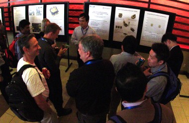
Poster Session
(Registration Required)
Poster Sessions are a great way to multitask during a
break, stretch your legs after a long session, and even network through
interaction with the poster presenters and other curious attendees. This
year’s session offers a variety of relevant topics that augment what you’ll
learn sitting in the general sessions.
"CSH Coating for High
Temperature"
Ichiro Fujishiro
Yamaichi Electronics
"Top Side
Probing on Handler"
Shaul Lupo
Intel Israel
“Auto Centering Manual Actuator One Manual Lid
for Different Package Sizes Testing”
Mah Ying Hoe
JF Microtechnology Berhad
Shamal Mundiyath
JF Microtechnology Berhad
“Novel Approach Of Enabling Customer Shadow EPROM
aka “EXTERNAL-EPROM” In HVM Environment ”
Maroon Maroon
Intel Corporation
Mouller Keren
Intel Corporation
Session 2
Test Tooling Made Easy
Whether you’re testing conventional packages like QFNs and BGAs, or emerging
2.5D and 3D packages, you’re only as successful as your test floor
equipment. This session’s presenters span the spectrum of tooling issues
beginning with a method for 3D package handling through the integration of
complex technologies. Next, you’ll learn how to prevent semiconductor test
system coolant leakage by implementing a hazardous warning system. Operator
error in manual test handlers comes under scrutiny thanks to a failure
analysis investigation in QFN packages. Lastly, we take a look at cost
saving through homogenous spring pin tip implementation in a high volume
manufacturing (HVM) environment.
(Registration Required)
"3D Package
Handling: A Simple Case of Integrating Complex Technologies"
Zain Abadin
Advantest America, Inc
"Innovation Way
to Prevent Semiconductor Test Tester Coolant Leakage with Hazardous
Warning System"
Yee Wei Tiang
Intel
ATM Penang,Malaysia
"Die-Cracking
Failure Analysis of QFN Packages in Manual Test Handler"
M.P. Divakar, PhD
Stack Design Automation
"Cost Saving
Through Homogenous Spring Loaded Pin Tip Implementation in High
Volume Manufacturing (HVM) Environment "
Chin Siang (David) Chew
Intel Technology
Nithya Nandhan
Subramaniam
Intel Technology
Chin Chien
Tee
Inerconnect Devices, Inc.
DESIGN
DAY
Tuesday, March 5, 2013
Session 3
Award Winning Performance
High
performance devices call for high performance test and burn-in solutions and
require participation by the entire test ecosystem including contactors,
sockets, the DUT board, along with the environment that testing takes place
in and the methodology applied. This session provides insight to each step
beginning with the development of a statistical model to identify the
optimized bandwidth for spring probes. Next up is a look at environmental
factors that can readily impact socket performance and thus indirectly test
yield. The third presentation verifies test methodology to troubleshoot a
device that is having issues in a very high performance test contactor to
determine the cause of the issues and affect changes to prevent them from
reoccurring. Lastly, we’ll hear about the unique challenges to create an
optimized test methodology for 25 to 40 GHz RF amplifiers, mixers, and down
converters in LFCSP (QFN) and WLCSP packages, considering connectivity
issues between DUT board and sockets.
(Registration Required)
"Design of
Experiments Using Spring Probe Parameters for Optimized Socket
Bandwidth"
Mike Fedde
Ironwood Electronics
Ila Pal
Ironwood Electronics
"Socket
Performance vs. Environmental Conditions"
Gert Hohenwarter
GateWave Northern, Inc.
"Troubleshooting
Test Oscillation Problems"
Jeff Sherry
Johnstech International
"Optimization of
Package, Socket, and PC board for 25 to 40GHz RF Devices"
Carol McCuen
R & D Circuits
Phil Warwick
R & D Circuits
Session 4
Bring
it to the Board (PCB)
The device under test (DUT) board is sometimes overlooked as a critical
element in test-and burn-in strategies. This session brings PCBs into the
limelight. The first presentation will cover some of the challenges that
various DUT layouts present, demonstrating to semiconductor and ASICS design
engineers the importance of considering final test hardware when designing
device layouts. Another important consideration, covered in the second
presentation, is the importance of performing RF characterization and
simulation in-house to accurately measure the materials’ electrical
performance.
As a bonus in this session, you’ll get a look at the
marketplace for test equipment and test consumables .
(Registration Required)
"Building
Optimized Test PCB’s Starts at the DUT"
Joe Birtola
CMR Summit Technologies
"High
Frequency PCB Material Characterization and Simulation"
Ryan Satrom
Multitest
Market Report
"Market Trends in Test Equipment
and Test Consumables "
John West
VLSI Research
Session 5
Better By Design
The greatest results always begin with a good design. In the world of test
and burn-in, the variations are endless. That’s why this session features a
broad assortment of design topics and perspectives. Beyond socket design,
we’ll learn about designing the right handler for the job. Next is a
birds-eye view of a socket’s creation from design concept to final assembly,
followed by a specific look at designs and applications for
package-on-package (PoP) device testing.
(Registration Required)
"A Novel Nested
Doll Concept in Universal Kit for Test Handler"
Yee Wei Tiang
Intel ATM Penang, Malaysia
"Anatomy of a Socket"
Paul F. Ruo
Aries Electronics, Inc.
"Special Designs and Applications for PoP Device Testing"
Siang Soh
Interconnect Devices, Inc.
Frank Zhou
Interconnect Devices, Inc.
James
Spooner
Interconnect Devices, Inc.
Khaled
Elmadbouly
Interconnect Devices, Inc.
Jon Diller
Interconnect Devices, Inc.
INNOVATIONS DAY
Wednesday, March 6, 2013
Session 6
And, at the Wafer Level
8:00 - 10:00
For many in the industry, performing final test at the wafer level is still
a novel idea. While providing some much needed solutions, it also comes with
its own set of challenges. The four papers in this session look at
wafer-level test from a number of different perspectives. The first one
discusses the mechanical and electrical differences between wafer-level
probe and wafer-level test using spring pins, focusing on requirements for
performing final test at the wafer-level. The second presentation provides a
comparison between traditional probe test for an RF wafer level chip scale
package (WLCSP) and a final test socket solution. TSV issues lead our third
author to share technologies that can bridge between 3D stacking and the 3D
IC without TSVs. Finally, we’ll gain insight into what some consider the
holy grail of burn-in and test – wafer-level burn-in (WLBI). Now that WLBI
is possible, it’s important to understand when it’s appropriate to consider
WLBI versus other burn-in alternatives.
(Registration Required)
"Spring
Probes and Probe Cards for Wafer-Level Test"
Jim Brandes
Multitest
"A Comparison of Probe Solutions For an RF WLCSP Product"
James Migliaccio
RF Micro Devices
"Bridging Between 3D and 3D TSV Stacking Technologies "
Belgacem Haba, Ph.D.
Invensas
"Wafer-Level Burn-in Decision Factors"
Steve Steps
Aehr Test Systems
Session 7
Product
and Material Mélange
This final session focuses on new products and materials in the test and
burn-in market. The first presentation looks at high-temperature burn-in
readiness, discussing a burn-in socket solution designed to address cost,
design and performance challenges of high temperature burn-in. Next on the
agenda is a description of new technologies developed to produce high
reliability stamped parts and elastomer contacts for a finer pitch and high
performance applications. The final presentation covers a new and innovative
ESD control molding compound for encapsulation, developed to reduce the ESD
issues in the test process.
(Registration Required)
"High
Temperature Burn-in (Up to 200 Deg. C): Are We Ready Yet?"
Noriyuki Matsuoka
Yamaichi Electronics Co., Ltd.
Kazumi Uratsuji
Yamaichi Electronics Co., Ltd.
Jec Sangalang
Yamaichi Electronics USA
Ryota Takeuchi
NGK Insulators, Ltd.
"Development of High Performance Spring Probe
Pin and Elastomer Contact by Stamping "
Samuel Pak
IWIN Co. Ltd.
A.J. Park
IWIN Co. Ltd.
"ESD Safe Materials for Test Socket and Encapsulation"
Tatsuya Kawasaki
Krefine Co., Ltd.
Awards
/ Closing Remarks(Registration Required)
It's been three days packed with
learning, exploring and sharing, but now it's time to pack our bags and
take what we've learned back to our jobs. But first, there are a few
closing remarks and some recognition to the people and papers that have
distinguished themselves in one way or another at BiTS 2013.
Watch the BiTS website for the posting of BiTS 2013
presentations, attendees, Exhibitor directory, photos, and for news about
BiTS 2014.
Page last modified
04/29/13
BiTS WorkshopTM is a production of
BiTS Workshop LLC