BiTS
is the world's premier workshop dedicated to
providing a forum for the latest information
about burn-in and test socketing, and related
fields.
At BiTS you'll find a comprehensive technical
program, exhibits of the latest products and
services, and many opportunities to meet,
network and explore ideas with other test and
burn-in socketing professionals.
Click here if you need the latest Acrobat(R) reader
from Adobe(R):
or
for an alternate free PDF
viewer, download the latest
Sumatra PDF
It is FAST!
ARCHIVE PAGES
COPYRIGHT NOTICE
The papers in this publication
comprise the proceedings of the 2011 BiTS Workshop. They reflect the authors’
opinions and are reproduced here as presented
with occasional minor edits. Their inclusion in
this publication does not constitute an endorsement by the BiTS Workshop, the
sponsors, BiTS Workshop LLC, or the authors.
There is NO copyright protection claimed by this publication; some tutorials may
be copyrighted.
However, each presentation is the work of the authors and their respective
companies: as such, it is strongly suggested that any use reflect proper
acknowledgement to the appropriate source. Any questions regarding the use of
any materials presented should be directed to the author/s or their companies.
All photographs on this page are copyrighted by BiTS Workshop LLC. The BiTS logo
and ‘Burn-in & Test Socket Workshop’ are trademarks of BiTS Workshop LLC.
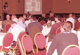
Technical Program
Authors from around the world shared their
latest work in 32 Papers and Posters covering a prominent
range of timely and fundamental topics.
A TechTalk session
was introduced, where Jon Diller of
Interconnect Devices shared
his deep knowledge of daily challenges with
the socket interface.
Jason Mroczkowski &
Ryan Satrom of Multitest, the Tutorial instructors, went in depth
as they delivered a comprehensive Tutorial focused specifically on ATE
hardware.
Invited Speaker, Al
Crouch, Chief Technologist of ASSET-Intertec, spoke on the goals of 3D
testing and the issues for making a “per die” test strategy for 3D package
structures.
Keynote Speaker, Roger
Schmidt of IBM described new technologies and best practices applied to thermal
control required in modern data centers, and described some thoughts on what the
future holds for power and cooling.
Fred Taber shared some
socket market data with BiTS participants mined from recent Fleck Research
research reports.
Finally, Brandon Prior of Prismark Partners
returned to BiTS to give attendees an update on the latest SiP packaging and
interconnect trends in his Market Update talk.
BiTS EXPO
2011
47 exhibitors, from socketing and related industries, exhibited their products and services
during breaks in the technical program. Click
HERE for the exhibitor list of BiTS EXPO 2011.
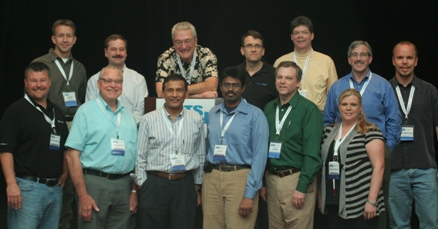
Participants
BiTS 2011 brought together well over 300 participants,
including nearly 250 full conference attendees, and 47 exhibitors from
around the world, representing end users and suppliers of sockets, boards,
burn-in systems, handlers, packages and other related equipment, materials and
services.
Front: Mark Murdza (Cascade Microtech),
Paul Boyce (Advantage Specialist),
Rafiq Hussain (AMD),
Ila Pal (Ironwood
Electronics),
Steve Hamren (Micron),
Kena Pegram (Phoenix Test Arrays)
Back: Morton
Jensen (Intel), Mike Noel (Freescale), Fred Taber (BiTS Workshop),
Valts Treibergs (Multitest),
Owen Prillaman (Tech-Connect Sales), John Hartstein (Wells-CTI),
Tim Swettlen (Intel)
Not pictured:
Joachin Moerbt (Advantest Europe),
Marc Knox (IBM), John Moore (Texas Instruments)
TUTORIAL
DAY
Sunday, March 6, 2011
TechTalk
Sockets: A Comprehensive, Comprehensible Guide to Contact Technology
This TechTalk provides a thorough survey of socket
technology that benefits attendees whether their involvement with sockets is
primarily commercial or technical.
Sockets are a niche within semiconductor test, yet they
present veterans, outsiders and newcomers with a daunting array of jargon and
assumptions. Challenged not only by the terms used to describe sockets and their
functions (which any glossary might address), but they are confronted with a
mythology about how sockets work and fail, which is often incomplete,
inaccurate, or misleading.
The TechTalk begins with a fundamental taxonomy of sockets,
separating them first by application among burn-in, characterization, and
automated functional test. Next, contact technologies are surveyed and
contrasted. All types of contacts are considered and compared, maintaining a
context of application throughout the discussion. This TechTalk considers not
only general classes of contacts (such as spring contact probes, rocking
contacts, etc.) but also specific design types within those classes (e.g.
three-piece spring contact probe designs versus conventional four-piece
designs).
With the building blocks defined, performance parameters are
then examined. The effect of contact geometry, materials, and cleaning methods
is summarized, and the general industry consensus, with respect to best known
practices is reviewed. The final section covers socket cost of ownership.
Mr. Diller is the
Director of International Sales & Marketing at Interconnect Devices,
Inc.. In his 15+ years of experience in applications engineering for
Interconnect Devices, Inc., Mr. Diller has worked around the globe on a
variety of test interconnect projects. He holds degrees from the
University of Iowa and Ottawa University.
Jason Mroczkowski
RF Engineering and Product Manager
Multitest
Ryan Satrom
Signal Integrity Engineer
Multitest
This
tutorial exposed the audience to the real world implications of
designing test hardware to meet various signal integrity and power
integrity needs. The tutorial started by defining the terminology
for analog and digital products. The tutorial thenl moved on to
present a range of past problematic designs showing real examples of
signal and power integrity failures. Armed with a common terminology
and previous experience, the tutorial moved into its main
section of providing the attendees with methods to design hardware
to meet both the power and signal integrity specifications. Topics
ranging from S-parameters, impedance targets, crosstalk, capacitor
and inductor fundamentals, measurement equipment, modeling equipment
and hardware selection were presented during the tutorial.
Mr. Mroczkowski is an
RF Engineering and Product Manager at Multitest. He has been with
Multitest for past 10 years, comprised of 5 years in Research &
Development and 5 years in Product Management. He is leading the
Multitest Simulation Services group which is focused on the integration
of simulation into the contactor and PCB design to delivery process
flow. Mr. Mroczkowski has published multiple articles on signal
integrity in semiconductor test, and regularly presents at tradeshows
including SVTest, IWLPC, Semicon and BiTS. He holds a patent for a high
speed interconnect design. He is pursuing an MBA and spends spare hours
with his wife and two boys age 3 and 1.
Mr. Satrom graduated
from Marquette University with a BSEE in 2004. Since then, he has worked
at Multitest as a Signal Integrity Engineer. He has presented at several
test industry conferences, including presentations at BiTS for the last
six years. He has also been published in WDPI magazine. His
presentations and publications focus primarily on signal integrity in
the test environment. His current responsibilities include high
frequency electrical characterization, RF contactor and PCB support, and
3D electromagnetic modeling.
The Industry wants to move to die stacking as the way to continue
keeping Moore’s Law valid. Form factor has been driving the trend for hand-held
and small-sized products by doing Package-on-Package and other externally
assembled 3D architectures.
The next logical step being worked on is to connect
bare-die to bare-die using Through-Silicon-Vias (TSVs). There are two different
drivers for TSV-based design: high-performance computing that can reduce the
size of complex microprocessor and graphic processors to increase yield and to
include different die functions made in different processes that can support
different voltages, but all done by one vertically integrated design house; and
the “competitive socket” where the space above a base-die can be filled by
multiple providers delivering die that implement the same function.
The
high-performance computing sector can custom design how they intend to test the
die and the stack and the final packaged device; but the competitive socket
sector has to have a successful test strategy that will “magically appear” when
disparate die are stacked and where each die regardless of provider will be
interoperable in a test sense with the other die in the stack.
In addition, the
test strategy must allow for wafer-testing and wafer-level burn-in, bare-die or
known-good-die testing, partial-stack testing, completed-stack testing, package
testing and must carry forward to allow debug-diagnosis, yield-analysis,
in-system, and field-return testing. The requirement is not to test to the level
to “throw away packages”, but to identify the die within a stack or the core
within a die — test is not effective without allowing feedback to fix a yield
problem.
This talk investigated the goals of 3D testing and the issues for
making a “per die” test strategy that can meet these conditions; and will
introduce the new IEEE Standard effort for 3D Test, P1838.
Mr. Crouch has been in DFT, Test, and Test-Automation for over
20 years and has worked at various industry IDM semiconductor companies such as
Texas Instruments, Digital, and Motorola before branching off into startups such
as Inovys (Low Cost ATE and Data-Analysis SW), DAFCA (Embedded Instruments and
Debug). Al Currently works for ASSET Intertech as the Chief Technologist for the
Core Instruments Division, where he drives Research & Development for tools and
methodologies related to Embedded “Inside the Chip” Instruments and the IJTAG
set of IEEE Standards (1500, P1687, 1149.7, and P1838). He has published
extensively at conferences, in journals, and for industry magazines; and is an
inventor on more than 15 Patents in the area of DFT and Test. He is most well
known for his Book on DFT for Embedded Cores and Digital Systems. Mr. Crouch
received his BSEE and MSEE from the University of Kentucky, and is a Senior
Member of the IEEE..
Recent surveys of CIO’s have shown
that energy is one of the leading concerns in the operation of data
centers. The IT industry ranks 6th in overall energy use compared to
other large industries, and if the manufacturing of IT equipment,
which ranks 11th, is included with the power required to drive all
the IT equipment, then this industry is 3rd on the list of
industries which use the most energy in the US.
The EPA issued a report to the US Congress in
August, 2007, as requested through the House of Representatives,
assessing opportunities for energy efficiency improvements to
computer servers and data centers in the United States. Two points
stand out in this report: 1) the infrastructure support of the IT
equipment within a data center contributes over one-half of the
overall power used for maintaining a data center, and 2) the rate of
growth of data center energy usage is significant.
Since that report a number of organizations have
created technologies and best practices that can improve data center
energy use significantly. There have been some significant
improvements made to data centers but much more needs to be done.
Some of the new technologies and best practices
applied to data centers are described in this talk, along with
some thoughts on what the future holds for power and cooling of data
centers, and how some of these will affect the design of servers of
the future. Data center technologies and best practices, which
include the deployment of co-generation, higher server ambient
temperatures, DC power, liquid cooling, and use of renewables, are described.
Dr. Roger R. Schmidt is an IBM Fellow, a National Academy of
Engineering Member, an IBM Academy of Technology Member and an ASME
Fellow.
He has over 30 years experience in engineering and engineering
management in the thermal design of IBM’s large scale computers, and
is IBM’s Chief Engineer on Data Center Energy Efficiency. At IBM he
has led development teams in cooling mainframes, client/servers,
parallel processors and test equipment, utilizing such cooling
mediums as air, water, and refrigerants. He now leads IBM’s lab
services team in providing customer support for power and cooling
issues in data centers.
Dr. Schmidt has published more than 100 technical papers and has
over 100 patents/patents pending in the area of electronic cooling.
He is a member of ASME’s Heat Transfer Division, and an active
member of the K-16 Electronic Cooling Committee. He has been an
Associate Editor of the Journal of Electronic Packaging and the
ASHRAE Research Journal and is now Associate Editor of the ASME
Journal of Heat Transfer.
He has taught Mechanical Engineering courses over the past 25
years to prospective Professional Engineers, and has given seminars
on electronic cooling and IT equipment power and cooling trends to a
number of organizations. He is past Chair of the ASHRAE TC9.9
committee on Mission Critical Facilities, Technology Spaces, and
Electronic Equipment. As part of TC9.9 he has been an instructor of
a number of workshops on data center best practices and energy
efficiency.
More and more, consumer electronics call for higher data rates and with
cloud computing appearing on the horizon, it’s only going to keep going up.
This poses challenges to the performance of standard contact technologies to
keep pace with further increasing frequencies. Speakers here presented socket
design parameters for improved signal and power integrity; an analysis of
the effects of impedance discontinuities; combining emerging technologies to
address high data rate challenges, and the impact of spring probe socket
geometry on high-speed IO channel performance. So go ahead, crank that
frequency up high, we dare you.
"Evaluation of
Contactor Impedance Mismatch on RF Performance "
James Migliaccio
RF Micro Devices
John Capwell
RF Micro Devices
"Contact
Optimization for Signal and Power Integrity "
Gert Hohenwarter
GateWave Northern, Inc.
"A Complete High
Frequency Interconnect Scheme for Testing >20Gb/s Interfaces "
Thomas P. Warwick
R&D Circuits
Thomas Smith
R&D Circuits
Dan Turpuseema
R&D Circuits
"Frequency-Domain
and Time-Domain Impact of Spring-Probe Socket Geometry on High-Speed
IO Testing "
Se-Jung Moon
Intel Corporation
Selim S. Akbay
Intel Corporation
Mustapha
Abdulai
Intel Corporation
Market Update
IC
Package Miniaturization and System in Package (SiP) Trends
This brief packaging market overview
presentation provides a perspective of overall IC package
trends. A short discussion on fine pitch leadframe packages, Wafer
Level CSP trends, and System-In-Package (SiP) evolutions such as
stacked die, Package on Package (PoP), and 3D TSV will provide a
global perspective of market sizes and adoption rates.
Mr. Brandon Prior joined Prismark Partners in 1996
and is the editor of Prismark’s Semiconductor and Packaging
Quarterly Report. He works with the leading component, equipment and
material providers to provide custom market and technology research
in the area of IC packaging. Mr. Prior earned BA and BE degrees from
Dartmouth College and the Thayer School of Engineering in Hanover
NH.
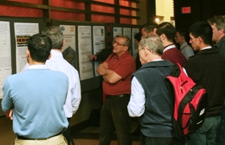
Sure, podium presentations are great, but sometimes it’s
nice to have a one-on-one chat with the author. And, we all wonder: how many
people are inclined to ask those provocative questions in front of the whole
audience?
With a variety of topics being addressed, poster sessions
offer the perfect opportunity for authors and attendees to interact directly
and even share ideas in an informal setting while enjoying some
refreshments.
"HVM Socket
Development for System Validation Boards, Featuring an Increasing
MTBF"
Shaul Lupo
Intel Israel
"A
Solution for a 26GHz, Tri-Temperature Test"
Ryan Satrom
Multitest
Paul Hurst
Multitest
"BGA
Interconnect Cres and Lifetime Characterization Methodology and its
Challenges"
Weida Qian
Intel Corporation
Jun Ding
Intel Corporation
Boon Tatt Gan
Intel Corporation
"High Force Hand
Socket Lid "
Chia Seong Lim
Test Tooling Solutions Group
“Does a Conductive Elastomeric Socket Have the
Same Electrical Performance as the Soldered Unit Attachment?”
Oren Ganon
Intel Corporation
“BGA Spring Probe for WLCSP (P0.4mm) - Multipoint
Contact to BGA”
Environmental issues such as lead-free materials, more complex
microprocessors and other sophisticated silicon devices have sent socket
designers back to the drawing board to come up with socket solutions that
match. In this session, learn about a lead-free contactor solution,
an air gap feature that extends a conventional test contactor beyond its
threshold, using embedded capacitance materials to improve sockets and test
boards & modulating socket dimensions to improve dual-core performance.
"New Contactor for Pb-free
Ball & NiPdAu Pad "
Jiachun
(Frank) Zhou
Interconnect Devices, Inc.
Kevin DeFord
Interconnect Devices, Inc.
Khaled
Elmadbouly
Interconnect Devices, Inc.
"Air Gap
Contactor "
Tuck Hon
Lam
Test Tooling Solutions Group
"Improving Test
Sockets and Test Boards Using Embedded Capacitance Material "
Mike Giesler
3M Company
Alexander (Sandy) Barr
3M Company
Yoshihisa
Kawate
Sumitomo 3M Ltd.
Yuichi Tsubaki
Sumitomo 3M Ltd.
"Improvement of
Dual Core Power Delivery Performance Through Modulation of
Socket-Mechanical Dimension "
This session addresses novel approaches to testing by enhancing test and
burn-in boards. We'll begin with a simple and low-cost PCB design that
recoups dielectric loss and enables high speed signal testing. Then you’ll
learn how two distinct methods for designing and manufacturing ATE final
test boards for fine pitch devices measure up. Next the benefits and risks
of high aspect ratio though hole vias in high density and fine pitch PCBs
used in the test interface will be discussed; and lastly, discover how using
embedded resistors ensures that all the ICs being tested see the required
voltage.
"Optimizing the
Motherboard for High Speed Signal Propagation"
Mustapha Abdulai
Intel Corporation
Erkan Acar
Intel Corporation
Anbinh Nguyen
Intel Corporation
"HDI vs High
Aspect Ratio CNC Drill for Fine Pitch Test PCBs"
Harsha Reddy
Gorilla Circuits
"Embedded Thin-Film NiP Resistors in Burn-In Trays"
Bruce Mahler
Ohmega Technologies, Inc.
"Benefits & Risks of
High Aspect Ratio Vias in ATE Boards"
Sometimes the issues are with the materials themselves, and sometimes it’s
what you’re trying to do with them. This session address both aspects of
materials for test purposes. Learn about a new electroforming
method for manufacturing small diameter barrels used in fine-pitch spring
probes. The next speaker will covered a novel pin material that helps reduce
solder migration. And the final presentation talks about tests for property
characterization of thin connector alloy strips.
"Electroformed
Barrels for Fine Pitch Test Probes"
Larre Nelson
Rika Denshi America
John Winter
Rika Denshi America
"Solder
Migration DoE for Pin"
Chen Yong Lai
Test Tooling Solutions Group
"Challenges
& Solutions For Characterization of Thin Connector Alloy Strip"
Occasionally no matter how hard you try, you just can’t pigeon-hole
brilliance. These varied presentations are linked by their very uniqueness
in the Test and Burn-in space. Prepare to be amazed as you hear about a
novel approach of using device-shaped probe structures placed inside the
socket; a prototype project intended to eliminate job interruptions caused
by burnt sockets and test boards; the continuation of last year’s PCB pad
wear analysis at 0.4mm pitch; and finally, some thermal testing insights
from the lab.
"Probing
Inside the Socket"
Marc Mössinger
Verigy
"Pin
Grid Array Current Sense Interposer Application Featuring Vertical
Embedded Resistors"
Shaul Lupo
Intel Corporation
Omer Vikinski
Intel Corporation
"PCB Pad
Wear Analysis at 0.4mm Pitch - the story continues..."
It seems repetitive and redundant, but it makes perfect sense. Before you
can use a socket, test board, etc, you need to know that they work
themselves. This session addresses various ways to "test the testers". Low
force contact technology for back-end test will be evaluated; learn
about a measurement system for determining the current carrying capacity of
contact springs; that's followed by an explanation of the benefits of
verifying socket functionality. This session then concludes with the
introduction of a simulation and design of experiment for improved
pin-to-pad alignment.
"Low
Force Contact Technology for Electronic Package Backend Test"
Jin Yang
Intel Corporation
Tim Swettlen
Intel Corporation
"Contact
Force Change As A Measure For Current Carrying Capability"
Marcus Frey
Multitest
"Testing
the Socket - The Benefits of Verifying Socket Functionality"
James Forster
Wells-CTI
Marco Michi
Wells-CTI
David Weston
Wells-CTI
Josef Magro
ST-Microelectronics
Silvio Spiteri
ST-Microelectronics
"Monte
Carlo Simulation and Design of Experiments for Improved Pin-Pad
Alignment"
Your facility may be equipped with state-of-the-art advanced test equipment
and use the most cutting edge technologies, but it means nothing if there’s
a glitch in the overall test floor operations. This session addresses issues
affecting the bigger picture; topics like navigating the hazardous waters of
coordinating and managing various operations to manufacture, assemble and
test ICs in multiple and remote locations, removing burrs and oil from
plastic socket casings and methodologies for automatically disabling
defective sockets.
"Product and
Test Security in a Remote Manufacturing Environment"
Don Richmond
Aehr Test Systems
"The Removal of Burr and Oil From Socket
Surface Using CO2 Jet Cleaning"
J. M. Lee
IMT Co. Ltd.
K. P. Lee
IMT Co. Ltd.
J. S. Choi
IMT Co. Ltd.
"Using Position Test History to Automatically
Disable Rogue Sockets"
It's been three days packed with
learning, exploring and sharing, but now it's time to pack our bags and
take what we've learned back to our jobs. But first, there are a few
closing remarks and some recognition to the people and papers that have
distinguished themselves in one way or another at BiTS 2011.
BiTS Award Winner
Summary:
Best Poster
“Does a Conductive
Elastomeric Socket Have the
Same Electrical Performance
as the Soldered Unit
Attachment?”
Oren Ganon - Intel
Corporation
Best Data
"PCB Pad Wear Analysis at
0.4mm Pitch - the story
continues..."
Valts Treibergs,
Christopher Cuda -
Multitest
Most Inspirational
"Probing Inside the Socket"
Marc Mössinger - Verigy
Best Paper – Tutorial in Nature
"Electroformed Barrels for
Fine Pitch Test Probes"
Larre Nelson, John
Winter - Rika Denshi
America
Attendee Choice
"A Complete High Frequency
Interconnect Scheme for
Testing >20Gb/s Interfaces"
Thomas P. Warwick,
Thomas Smith, Dan
Turpuseema - R&D
Circuits
Best Paper
"Improvement of Dual Core
Power Delivery Performance
Through Modulation of
Socket-Mechanical Dimension"
Suchismita Ghosh, Jeremy
D. Littrell, Satish
Prathaban - Intel
Corporation
Page last modified
03/22/12
BiTS WorkshopTM is a production of
BiTS Workshop LLC