
Virtual Event - November 1-4, 2022
| Tuesday | November 1, 2022 - 0900 to 1130 Shanghai/CST |
|---|---|
| Wednesday | November 2, 2022 - 0900 to 1130 Shanghai/CST |
| Thursday | November 3, 2022 - 0900 to 1130 Shanghai/CST |
| Friday | November 4, 2022 - 0900 to 1130 Shanghai/CST |
Event registration is free courtesy of our sponsors
TestConX has, over the course of its twenty two-year history, established itself as the preeminent event for test consumables, test cell integration, and test operations. The program scope has expanded over these years from packaged semiconductor “final” test and burn-in to encompass all practical aspects of electronics testing including validation, advanced packaging testing, system level test, module test, and beyond to finished product test.
Last year, the 7th annual TestConX China 2021 was held as a virtual live on-line event with excellent presentations and question and answer sessions. We will once again hold TestConX China 2022 as a virtual event using the same online platform. This will provide global attendees with the opportunity to see new locally created and developed content in addition to the best from international presenters.
Don’t miss this opportunity to be part of TestConX as we connect a larger community of test professionals and to participate in this excellent event!
Tuesday
November 1, 2022 - 0900 to 1130 Shanghai/CST
Ted Wan is Vice Chair and Executive Committee member, BritCham Shanghai and President, greater China and Executive Committee member of Smiths Group plc. Ted is a seasoned corporate executive. He has diverse industrial and automotive background in his past 20+ years’ experience serving leading global companies including JD Power, Danaher, Stanley Black & Decker, and Smiths Group with responsibility for growing their China business. Ted has extensive experience and a strong track record in growing business in China in the Industrial and Automotive markets.
Borne and brought up in Beijing, Ted and his family have lived in Shanghai for over 12 years. He now chairs British Chamber’s Advanced Engineering and Manufacturing committee. Ted’s leadership philosophy is “The only way to make BIG things happen it to taking people with you.” His leadership style, rich industry background and extensive global and China local networks will bring great value to British Chamber of Commerce Shanghai and its members.
万江作为英国上海商会副主席和行政管理委员会成员及史密斯集团全球行政管理委员会成员和史密斯集团大中华区总裁是一个经验丰富的公司行政主管。
他服务于J.D. Power、 丹纳赫集团、史丹利百得、史密斯集团等领先的全球性企业,并有着20多年的工业和汽车行业背景。他致力于帮助这些企业制定中国区战略并推动在中国的业务增长。万江在中国的工业及汽车市场拥有丰富的经验和卓越的业绩增长记录。
万江出生并成长于北京,目前他和他的家人已经在上海生活超过12年。他目前还是英国上海商会先进工程及制造业委员会主席。万江的领导力哲学是 “推动实现重大事项需要大家共同的努力“。他的领导风格,丰富的行业背景和广泛的全球及中国市场资源及网络将给英国上海商会及其会员带来极大的价值。
“机器学习可以如何在硅后验证/生产阶段帮助客户 ”
Abstract - Biography (English)
With the chip design becoming more and more complex, Post silicon validation which is a key process before mass production, is facing many challenges, such as tight schedule, validation difficulty of complex chips, and high requirements for chip quality/performance, etc. A better method is needed to solve the above problems. This paper introduces a methodology based on machine learning algorithm, which can automatically generate test conditions for related tasks of post-silicon validation based on a constrained random way. Compared with the traditional shmoo, it improves the coverage and execution efficiency. The unique variable selection feature can help users quickly find out the correlation between input and output, and machine learning algorithms can help users to tune and debug the chip, so that the chip can achieve the best performance and speed up the chip Time to market. We are also exploring the scenario that this methodology is used in the production test phase, how to effectively eliminate the impact of uncertainty caused by the introduction of a large number of external production process parameters on the robustness of mass production test program.
Business Development Manager of Advantest (China), mainly responsible for the promotion of AI-based data analyze solutions for validation. As the business owner of the company's new artificial intelligence products, he is committed to promoting the company's leading edge in business.
摘要 - 简介 (Chinese)
在芯片设计越来越复杂的当下,作为量产前的关键流程的PSV,面临着诸多挑战,例如紧张的时间表,复杂芯片的验证难度,对芯片质量的高要求等,需要一种更好的方法来解决以上的问题,本文介绍了一种基于机器学习算法的方法,可以基于受约束的随机方式自动为硅后验证的相关任务生成测试条件,与传统的Shmoo方式相比提高了覆盖率,增加了执行效率. 特有的变量选择的功能可以帮助用户快速找出输入对输出的相关性,机器学习算法可以帮助用户对芯片进行调优和调试,让芯片达到最佳性能的同时加快了芯片推向市场的时间. 我们也在探索此方法论用在生产测试阶段的场景,怎样有效的消除因为大量外部生产工艺参数引入造成的不确定性对量产测试程序鲁棒性的影响
爱德万测试(中国)管理有限公司 业务发展经理,主要从事推广用于验证的AI大数据分析解决方案. 作为公司人工智能新产品的业务负责人,致力于推进公司业务的领先优势.
“ETS-800 平台的阈值测试方法总结介绍”
Abstract - Biography (English)
Threshold tests are very common for testing most of the devices, there are several types of threshold tests, and two main types of test method known as step search and binary search. This presentation mainly introduces some different step search methods as implemented on Teradyne ETS-800 platform, and compare them in view of test time, PTE (parallel test efficiency), repeatability, the difficulty of coding and debugging and so on. In the end, we also have a brief introduction about Threshold Step Search Code Library combining all these test methods into a single test function, which makes our code development and debug process easier and more flexible.
Cham Li, Application Engineer in Teradyne. 10 years’ experience in ATE testing, focus on SOC, PMIC and automatic test solutions.
摘要 - 简介 (Chinese)
阈值测试是一种在很多的芯片测试中都很常见的测试项,有一些不 同类型的阈值测试, 和两种主要的测试方法类型被称之为逐步搜索 和二分法搜索。 本文基于泰瑞达的ETS-800测试平台主要介绍一些 不同的逐步测试方法, 并从它们的测试时间、并行度、 稳定性、 编程调试的难易程度等方面进行比较。最后, 我们会简单介绍下阈 值逐步测试代码库,它把所有不同的测试方法集成到一个单一的测 试函数, 这使我们的代码开发和调试过程变的更加简单和灵活。
李崇明, 应用开发工程师,泰瑞达(上海)有限公司。10年的ATE 测试开发经验。主要从事SOC,电源管理芯片,汽车电子类芯片的 测试解决方案开发。
Wednesday
November 2, 2022 - 0900 to 1130 Shanghai/CST“插座供应商连续第二年竭力满足客户需求 ”
Abstract - Biography (English)
Sales of semiconductors exceeded $550B in 2021 and are on track to grow at double-digit growth rates in 2022 despite concerns about rising inflation, global recession, trade wars, and the conflict between Russia and Ukraine. Suppliers of burn-in and test sockets have struggled to keep up with both the high levels of demand and technical challenges. In fact, sales in 2021 would have grown much more than the 19% reported if suppliers were not constrained by a lack of materials, people, and manufacturing capacity. It looks like 2022 is going to be a great year for revenues but many of the supply chain problems have not been resolved. Lead times for raw materials are not getting shorter, prices are increasing, and end users are still experiencing delays in the delivery of sockets. Now, more than ever, it is important to keep track of what is happening in the market. This presentation will provide an overview of the current market situation, which fast-growing segments to watch out for, and what suppliers can do to benefit from the fast-changing environment.
Lin Fu is a Principal Analyst in the Semiconductor Subsystems and Test Division at Yole Intelligence. Lin’s mission is dedicated to test essentials related activities by providing market & technology analyses along with consulting services to semiconductor industry players. Lin has a bachelor’s degree from the University of Edinburgh and a PhD degree from the University of Cambridge. Before joining Yole, Lin was engaged in semiconductor technical and market research for 5 years in VLSIresearch.
摘要 - 简介 (Chinese)
2021年半导体工业的销售额超过5500亿美金,2022年预计仍会有双位数增长,尽管一些不确定因素的存在,如:不断上涨的通货膨胀,全球性经济衰退,贸易争端,俄乌军事冲突等。 老化座及测试座供应商一直在努力跟上高市场需求和解决技术挑战。事实上,如果供应商不受材料、人员和制造能力不足的限制,2021 年的销售额增长将远远超过19%。2022 年预计市场会持续增长,但诸多供应链问题尚未解决。原材料的交货时间并没有缩短,价格继续上涨,而终端客户仍在经历插座交付的延迟。 现在,相较以往任何时候,跟踪市场动态变得尤为重要。 本演讲将概述当前的市场情况,需要注意哪些快速增长的细分市场,以及供应商可以做些什么来从快速变化的环境中受益。
付琳是Yole Intelligence半导体子系统与测试部门的首席分析师,主要负责为半导体从业者提供 测试耗材相关的技术与市场分析、咨询。付琳拥有爱丁堡大学电气工程学士学位和剑桥大学博士 学位。加入 Yole 之前,付琳曾在 VLSIresearch 从事了 5 年的半导体技术和市场研究工作。
“Air over stub 对于 56Gbps Serdes 和 mmWave的影响及优化 ”
Abstract - Biography (English)
High frequency applications (e.g. 56Gbps Serdes, mmWave) keep challenging the PCB manufacturing capability and simulation accuracy. Via is a common structure on PCB (application and test board, etc…), and via stub loss will do effect on the high frequency signal quality for any usage. This presentation will analyze the impact of via stub loss to the 56Gbps Serdes and mmWave signals, then introduce the high frequency SI improvement by air over stub, and gives recommendation for PCB manufacturing process and simulation consideration.
Chenrui received master’s degree from Tongji University, Shanghai in 2012. He began his career as a HW design engineer in Teradyne, Shanghai. In the first 5 years, he supported some famous customers like TI, BOSCH, STM etc., as an ATE Loadboard hardware designer. In the last 5 years, focused on signal & power integrity simulation and has provided HW solution for many kinds of chip successfully.
摘要 - 简介 (Chinese)
随着终端需求的发展,高频信号的应用(如 56Gbps Serdes, mmWave, …)一直在挑战着PCB的制造能力,并且对信号仿真精度要求越来越高。Via是PCB(应用板,测试板,…)的常见结构,并且Via的stub对任何高频的信号质量都有直接的影响。本文将分析Via stub对于56Gbps Serdes, mmWave信号的影响,介绍通过优化via stub带来的高频SI性能提升,并且会给出PCB生产流程以及仿真模型的相关建议。
陈锐,2012年于上海获得同济大学硕士学位。毕业之后,作为一名硬件设计工程师在泰瑞达(上海)开始了他的职业生涯。在工作的前5年,从事ATE Loadboard PCB硬件设计工作,服务过TI, BOSCH, STM等知名客户。最近的5年,他专注于信号和电源完整性仿真,成功为许多种类的芯片提供了硬件解决方案。
“实现2ps/inch差分对内延迟的112G PAM4设计”
Abstract - Biography (English)
For differential pair, intra-pair skew can degrade its performance depends on how serious the skew is. So, length matching within a differential pair is always required when doing 112Gbps PAM4 design. However, even perfect length matching (<1mil) does not equal to 0 skew if fiber weave effect is not considered. This topic first introduce how intra-pair skew can degrade the performance briefly. Then, we explain how fiber weave effect can result in >10ps/inch skew by theory, simulation and test. Finally, we discuss 4 mitigating methods for glass fiber skew, the first method is using high spread out glass fabric, the idea of it is minimize dk difference inside dielectric material. The second method is CAM file rotation, the idea of it is balance dk variation between P&N in a differential pair. The third method is using 2 ply core and PP when design a stack up, the idea of it is also minimize dk difference inside dielectric material. The last method is using low-dk glass fabric, the idea of it is reduce dk gap between glass and resin. Simulation and test are also implemented to verify all these 4 methods. By using method 1 and 3, intra-pair skew can be reduced to 2ps/inch.
Zhi-Peng Lu received master’s degree from Southeast University, Nanjing in 2016. He began his career as a HW design engineer in Teradyne, Shanghai. In past 5 years, he focused on signal & power integrity simulation and has provided HW solution for many kinds of chip successfully, such as DDR, MCU, application processor, AI, HPC, network switch and so on.
摘要 - 简介 (Chinese)
对于差分信号,差分对内延迟差直接影响到信号质量的好坏。所以,对于112Gbps PAM4设计,差分对内等长的要求必不可少。然而,如果不考虑玻纤效应的影响,即使差分对内等长配到1mil之内,差分对内延迟差依然不会等于0ps。本文首先简要说明了差分对内延迟是如何影响其信号质量的。然后,本文从理论、仿真和测试几个方面,说明了玻纤效应为何会导致大于10ps/inch的延迟。最后,本文讨论了4种优化玻纤效应延迟的方法:第一种是采用使用扁平开纤玻璃布的板材,其核心思想是减小板材内部dk值的差异;第二种方法是旋转CAM文件或者走线,其核心思想是平衡差分对内,即P/N之间的dk波动;第三种方法是采用2 ply的PP和Core来设计叠层,其核心思想也是减小板材内部dk值的差异;第四种方法是采用具有low-dk特性的玻璃纤维布,其核心思想是减少玻璃布和树脂之间dk值的差异。本文对上述四种方法进行了仿真验证,并且通过测试证明,在同时采用方法1,2,3之后,差分对内延迟可以减小到2ps/inch。
卢致鹏,2016年于南京获得东南大学硕士学位. 毕业之后,作为一名硬件设计工程师在泰瑞达(上海)开始了他的职业生涯,过去5年,他专注于信号和电源完整性仿真,成功为许多种类的芯片提供了硬件解决方案,比如内存颗粒, 微控制器, 应用处理器, 人工智能芯片, 高性能计算芯片, 网络交换机芯片等等。
“Power-On-Reset (POR) 验证平台 ”
Abstract - Biography (English)
Today, there's no automated tools that help root cause and find these electrical specification violations. The validation activities from the first build of the board to product ready to be shipped take about 7-10 weeks. There are many limitations in the process which could not be done during pandemic time such as on-site debug and testing of the platform due to quarantine and workforce reduction. Apart from that, the global shortage of silicon that caused by pandemic has resulted business running slow and halted at some point . Consequently, engineers have limited access to boards and silicons to perform debug and validation. To ensure product development without disruption, Intel created an innovative small form factor tool that can be controlled with cloud-based remote debug infrastructure. The tool is called Power-On-Reset (POR) tool that can be fully configurable to collect and timestamp electrical activities across several signals over a specific period of time. It then compares the collected data to a set of expected behaviors downloaded to the tool. The expected behaviors are defined as “scripted" electrical specs (rule kits). The integrated rule-checking software capability of the tool automates time consuming and expensive debug and validation processes through the push of a few buttons. This greatly improves the user experience and simplifies its operation. The results collected are displayed on a user-friendly GUI in less than one minute with remote debug capability enabled by the cloud-based infrastructure. There is minimum to none learning curve to use this tool. The remote debug cloud services can be accessed with proper authentication. The POR Tool solution comprises of four steps, (1) Documented specifications are converted to Scripted Rule Kits. (2) User downloads rule kits to the POR Tool hardware. (3) All digital and analog behaviors collected by the tool. (4) Pass and fail results reported “instantly” to the GUI. At this point, the POR Tool captures and compares power-on-reset sequences from Intel platforms and then reports all spec compliance and violations within 60 seconds. The solution significantly reduces the debug and validation engineering man hours, accelerates product time to market, and promotes customer self-sufficiency.
Dr. Angie See Tien Ng is an AI Principal Engineer from Intel who pioneer Cloud based Remote Debug (CBRD), System Cloud for University (SC4U) and spearheaded AI Virtual Chat Bot. She has been in Intel for 13 years and in the industry for 25 years. (IQ Group, Altera, Intel) Her career includes R&D electronics design, RF designer, FPGA IC characterization, Electrical Validation, Functional Safety, IOT Customers Enabling and Design-In. Angie always passionate in innovation and is honoured with Distinguished Invention Award by Intel. She graduated from Campbell University with BEng in Microelectronics/Physics and obtained Master in Engineering (1st class) in 2014 from Multimedia University major in Microelectronics. In 2021, she completed Doctorate in Multimedia Technology with USM (University Science Malaysia) in the area of designing cloud-based virtual learning & testing for industry.
Amyrul Azuan Mohd bahar received his BSc degree in Electronic Engineering from Universiti Teknikal Malaysia Melaka, Malaysia and obtained his Doctorate from the same university in 2017 in the field of Microwave Engineering. He registered as IEEE Graduate member in Institute of Electrical and Electronics Engineers and IEEE Microwave Theory and Techniques Society. His current R&D interests include microwave/RF applications, sensor design, and power embedded system technology. He joined Intel Microelectronics (M) as a Sr. platform power engineer in 2017 until present.
Yean Shim Tan received his BSc Degrees in Computer Systems Engineering in 2006. He is currently working in Intel Microelectronic, in the Internet of Things Group as Cloud Based Remote Debug Engineer. Team lead for Intel Pre-PRQ products, responsible to provide technical support and remote platform enabling to customer.摘要 - 简介 (Chinese)
目前,没有自动化工具可以帮助找到不符合电气规范的根本原因。 从首次构建电路板到准备发货的产品的验证活动大约需要 7-10 周。 由于疫情期间,因为隔离政策的限制和人力短缺,验证过程中有许多程序无法完成,例如现场调试和平台测试。 除此之外,由于疫情引起的全球矽晶片短缺导致业务运行缓慢或暂停。 因此,工程师只能用有限的方法与时间来执行调试和验证电路板及芯片。
为确保产品开发不受干扰,英特尔创建了一种创新的小型工具,可以通过云端的远程调试基础设施进行控制。 该工具称为上电复位 (POR) 工具,可以完全配置为在特定时间段内收集多个信号的电气活动并为其加上时间标示。 然后,它将收集的数据与下载到该工具的一组预期行为进行比较。 预期行为被定义为“脚本化”电气规范(规则套件)。 该工具的集成规则检查软件功能通过按几个按钮,自动执行耗时且昂贵的调试和验证过程。 这极大地改善了用户体验和简化其操作。 收集的结果在不到一分钟的时间内显示在用户友好的 GUI 上,并通过云端的基础设施启用远程调试功能,使得使用此工具的学习曲线到最少甚至没有。 进入远程调试云端服务,须通过适当的身份验证方可执行。
POR 工具解决方案包括四个步骤,(1) 将文档化规范转换为脚本化规则套件。 (2) 用户将规则套件下载到 POR 工具硬件。 (3) 所有数字收集的和模拟行为皆由工具执行。 (4) 通过和失败结果“立即”报告给 GUI。 此时,POR 工具会捕获并比较来自英特尔平台的上电复位序列,然后在 60 秒内报告所有规范合规性和违规行为。 该解决方案显著减少调试和验证工程工时,加快产品上市时间,并可推广至客户端自行使用。
Angie See Tien Ng 博士是英特尔的 AI 首席工程师,他开创了基于云的远程调试 (CBRD)、大学系统云 (SC4U) 并率先推出了 AI 虚拟聊天机器人。 她在英特尔工作了 13 年,在这个行业工作了 25 年。 (IQ Group、Altera、英特尔)她的职业生涯包括研发电子设计、RF 设计师、FPGA IC 特性分析、电气验证、功能安全、IOT 客户设计导入。 Angie 一直热衷于创新,曾荣获英特尔颁发的杰出发明奖。 她毕业于坎贝尔大学,获得微电子/物理学士学位,并于 2014 年获得多媒体大学微电子专业工程硕士学位(一等)。 2021 年,她获得了 USM(马来西亚科学大学)的多媒体技术博士学位,研究领域是工业设计基于云端的虚拟学习和测试。
Amyrul Azuan Mohd bahar毕业于马来西亚马勒卡大学(Universiti Teknikal Malaysia Melaka),获得电子工程学士学位,并于2017年获得该大学微波工程领域的博士学位。他在电气电子工程师学会和电气电子工程师学会微波理论与技术学会注册为IEEE研究生会员。他目前的研发兴趣包括微波/射频应用,传感器设计和电源嵌入式系统技术。他于2017年加入Intel Microelectronics (M),担任高级平台电源工程师。
Yean Shim Tan于2006年获得计算机系统工程学士学位。他目前在Intel微电子工作,在物联网组担任基于云的远程调试工程师。领导英特尔Pre-PRQ产品的团队,负责为客户提供技术支持和远程平台。
Thursday
November 3, 2022 - 0900 to 1130 Shanghai/CST“COVID-19全球大流行对半导体超需求和测试成本的影响”
Abstract - Biography (English)
During the last two years of the pandemic, Semiconductors have proven to be vital to the well-being of the world and economic growth. As a result, semiconductor manufacturing has experienced a hyper-growth environment. During this period, the cost of semiconductor manufacturing has increased substantially. The cost increases are very clear in wafer fabrication, but this presentation will explore how the cost of Test has trended during COVID-19 and before, with a special emphasis on Test Connectivity systems such as Sockets and Probe Cards. As part of the presentation, the semiconductor and test forecasts are presented in light of the world entering into a post-COVID-19 era.
Panchami is a Market Research Analyst at TechInsights. Her primary focus is Test Connectivity Reports such as Probe Card, Sockets and Device Interface Boards. Part of her work focuses on the market analysis of semiconductor test both in Memory and Non-memory markets.
She graduated from California State University, Channel Islands majoring in Mathematics. She also has an MBA in Finance from Ramaiah Institute of Technology, Bangalore. She has published a Master Thesis about using Markov Chain and Python to analyze and predict the Stock Market trend. Panchami has also published (5) many academic papers in Indian Research Journal, SAGE Student Research Conference, etc.
摘要 - 简介 (Chinese)
在COVID-19全球大流行的最后两年,半导体已被证明对世界福祉和经济增长至关重要。因此,半导体制造业经历了一个高速增长的环境。在此期间,半导体制造成本大幅增加。晶圆制造的成本增加非常明显,本演讲将探讨测试成本在 COVID-19 期间及之前的趋势,特别强调测试系统,如插座和探针卡。作为演讲的一部分,半导体和测试预测是根据世界进入COVID-19后时代的条件。
Panchami 是 TechInsights 的市场研究分析师。 她的主要工作是著重于测试硬体连结介面的报告,例如探针卡、元件测试座和测试介面转接板。 她的部分工作则专注于记忆体和非记忆体半导体测试的市场分析。
她毕业于加利福尼亚州立大学海峡群岛分校,主修数学。 她还拥有班加罗尔拉迈亚理工学院的金融 MBA 学位。 她发表了一篇关于使用Markov Chain 和 Python 进行分析和预测股市趋势的硕士论文。 Panchami 还在 Indian Research Journal、SAGE Student Research Conference 等发表了 (5) 多篇学术论文。
“高功率散热下晶圆温度测试的新方法 ”
Abstract - Biography (English)
It is well-known that the temperature of a chip increases when power is applied. A common method to keep the temperature under control while the chip is tested is to work with a temperature offset. But using an offset is only valid for static power application, for example test with constant 600W power dissipation. However, this is not the typical case; it is more typical that a strongly fluctuating, very dynamically changing power loss is generated during the test. Therefore, a method will be presented, which allows an evaluation of the behavior of a chip under these dynamic conditions before the actual test. The big advantage of this method is its independence from both tester and product. The solution is based on our ProbeSense™ calibration tool, which in this case is extended by a power generating element. This power element, which functions as a kind of heater, can simulate the exact expected dynamic power input during testing. Sensors are placed in the ProbeSense™ and in the chuck to gather the relevant temperature data. With a new, unique software the dynamic test can be simulated and the expected temperature behavior of the device under test (DUT) can be shown. The new feature is that this can be done with the parameters of the original test program. So the user is now able to predict the temperature behavior of the DUT long before the test and long before the expensive investment into tester or the long waiting time for the first silicon. Parameters like the reachable guard band for accuracy, peak temperature, or how to target junction temperature, and, last but not least, the suitability of the thermal chuck, will be known ahead of the test set-up. The tool, software, and performance data will be presented, and a newly developed liquid high-performance chuck will also be introduced. Thanks to a unique new concept, the liquid chuck can maintain accurate temperatures under dynamic power dissipation of the DUT.
Xiang “Joshua” Zhou has a Bachelor Degree from Huazhong University of Science and Technology and a Master Degree in Communication Electronics from Tsinghua University. After graduation, he worked for Texas Instruments Incorporated for 11 years and then served as the vice president of operations and sales for a well-known semiconductor design company in China. In 2018, Mr. Zhou Xiang joined ERS electronic GmbH-a German Semiconductor Manufacturer-and was appointed as Vice President in March 2021. With his more than 20 years’ experience in semiconductor industry, Mr. Zhou successfully leads the ERS Greater China team to introduce ERS’s thermal management solutions for wafer probing and advanced packaging technologies to the Chinese Market.
摘要 - 简介 (Chinese)
众所周知,芯片通电之后,温度会升高。常见的对在测芯片进行温度控制方法是温度补偿,但 这种方法仅适用于静态功率应用,比如恒定 600W 功率耗散测试。但这种测试并不典型,更普 遍的情况是在测试过程中功耗产生强烈的波动,即动态变化。 因此我们将介绍一种方法,它允许在实际测试前,在动态环境下对芯片进行评估。这种方法的 最大优势是它将独立于测试机和产品。
该解决方案是在我们的校准工具 ProbeSenseTM基础上,通过施加一个功率元件而开发的。该 功率元件发挥着类似加热器的功能,可以在测试过程中模拟确切的预期动态功率输入值。 ProbeSenseTM和卡盘内部都装载有传感器,以收集相关温度数据。 通过利用一个全新的、独特的软件,可以模拟出动态测试并同时显示出被测设备(DUT) 的预期 温度变化。它的独具一格之处在于,这个过程可以通过原始测试程序参数来完成。因此,用户 可以在测试前很长一段时间里,在投资昂贵的测试机到位之前或是在等待首个硅片时,即可预 测出 DUT 的温度变化。诸如可达精确程度的阈值、峰值温度或是如何达到结温等参数,乃至 于温度卡盘的实用性,都将在开始测试之前被掌握。 本次演讲中将会介绍相关工具、软件以及性能参数,另外还有一个全新开发的、特殊的高性能 温度卡盘。受益于该独特的全新概念,该卡盘可以在 DUT 动态功率耗散的情况下保持温度的 准确性。
周翔先生本科毕业于华中科技大学,2000年取得清华大学通信电子工程专业硕士学位。毕业以后,曾供职于美国德州仪器公司长达11年之久,随后在国内一家知名半导体设计公司担任运营、销售副总经理。 2018年,周翔先生加入德国半导体制造商ERS electronic GmbH公司,并于 2021年3月被正式任命为公司副总裁。凭借着在半导体产业积累的20多年的经验,周翔先生带领ERS大中国团队,将ERS的晶圆测试、温度控制、以及先进封装技术,成功的引入中国市场。周翔先生本科毕业于华中科技大学,2000年取得清华大学通信电子工程专业硕士学位。毕业以后,曾供职于美国德州仪器公司长达11年之久,随后在国内一家知名半导体设计公司担任运营、销售副总经理。 2018年,周翔先生加入德国半导体制造商ERS electronic GmbH公司,并于 2021年3月被正式任命为公司副总裁。凭借着在半导体产业积累的20多年的经验,周翔先生带领ERS大中国团队,将ERS的晶圆测试、温度控制、以及先进封装技术,成功的引入中国市场。
“基于爱德万测试V93000 测试平台实现的具有挑战性的汽车电子测试方案的设计以及应”
Abstract - Biography (English)
Worldwide automotive semiconductor manufacturers, such as Infineon, NXP and Bosch, are accelerating their next breakthrough automotive design for advanced driver assistance systems, in-vehicle networking, body, chassis, powertrain and safety applications. Meanwhile the epidemic and new energy and intelligent connected vehicle technology development, car chip shortage has impact on the automotive industry, snarling supply chains around the world and severely hampering the vehicle production. Thus, as one important ATE supplier, we will face some testing challenges like the high parallelism?low cost control?test time and different types automotive devices from the semiconductor manufacturer under the current conditions, which also inevitably bring with higher requests for tester, instrument and test solution. Although some traditional solutions have been applied in the testing, but it can’t meet the special or extreme condition, so some special or innovative solutions will be designed in the load board and testing application. This paper will introduce the solutions from some real cases which have been successfully applied to the customers production projects and gotten a good performance. Details will be discussed in following aspects:1 Automotive electronic classification and challenges2 Floating resources innovative using3 PS1600 HV novel using with low and high voltage instrument connections 4 Systematic utility solution, utility control bit extension and power analysis5 Quality and safety software check tool application In conclusion, these systematic solutions from hardware to software are significant in PAC devices, which can be applied for other similar test scenarios and will be of certain reference significance in future.
Kaitao Liu, from Global ADC, senior engineer. Joined Advantest China in 2016, work scope included test solution design for automotive and sensor chips, test program development and consulting with the top semiconductor companies for a long time.
摘要 - 简介 (Chinese)
全球汽车半导体制造商,像英飞凌、恩智浦和博世等,正在加速他们的下一代汽车电子技术的发展,包括先进的驾驶辅助系统、车内网络、车身、底盘、动力系统和安全应用。与此同时,新冠疫情的肆虐,以及新能源和智能车联网技术的发展,都加重了汽车芯片的短缺,从而对汽车行业造成冲击,使全球供应链陷入混乱,汽车生产受到严重地阻碍。 因此,作为全球领先的半导体测试设备供应商,我们将不得不面对半导体厂商在当前缺芯大环境下的下提出的高并行度、低成本、较短的测试时间等要求,并且要能够同时满足不同类型的汽车电子芯片测试等方面的挑战,这也不可避免地对测试机、板卡和相应的测试解决方案提出了更高的要求。虽然一些传统的解决方案已经应用于量产测试中,但它并不能完全满足当前较高的测试要求或者一些特殊的应用条件,因此在负载板和测试方案的设计中会提出一些新的解决方案。 论文主要介绍一些来自于真实案例的解决方案,这些方案都已经量产并且取得了较好的性能。论文主要讨论一下方面: 1 汽车电子的分类以及挑战 2 浮点资源的一些新颖的使用 3 测试中高低压板卡的连接,保护电路以及实际案例 4 系统性的relay方案,以及utility bit的扩展以及功率的分析 5 质量相关的检查工具的使用 总之,这些从硬件到软件的系统性解决方案对于PAC 类的芯片有比较重要的意义,同时希望能够给类似的芯片能够提供一些参考。
刘凯涛 隶属于爱德万测试全球应用开发中心,高级工程师。2016年加入爱德万测试中国,主要负责汽车电子芯片和传感器类芯片测试方案的设计,测试程序的开发以及相关的咨询工作,长期与行业顶尖的半导体公司进行项目的开发以及管理工作。
“聊天机器人中的 RMT”
Abstract - Biography (English)
We have begun development on the integration of RMT tools into QIRI chatbot in Teams. The RMT, also known as Rank Margin Tool, is a tool built with the purpose to generate, calculate and report out the system memory interface cold-boot DDR training result of timing and voltage margins. To run it locally, users will need to download the original RMT tool, which is a built-in excel macro that output a table within the excel file. By integrating it into QIRI chatbot, user can skip this step entirely. The user can provide the QIRI chatbot the log file required to output the cold-boot DDR training result, in which the QIRI chatbot will automatically run the RMT on its own end, and then return the output information back to the user. This QIRI integration not only provides the users with easy accessibility to the RMT, it also allows user to get the result without requiring the users to wrangle with the RMT tool itself.
Dr. Angie See Tien Ng is an AI Principal Engineer from Intel who pioneer Cloud based Remote Debug (CBRD), System Cloud for University (SC4U) and spearheaded AI Virtual Chat Bot. She has been in Intel for 13 years and in the industry for 25 years. (IQ Group, Altera, Intel) Her career includes R&D electronics design, RF designer, FPGA IC characterization, Electrical Validation, Functional Safety, IOT Customers Enabling and Design-In. Angie always passionate in innovation and is honoured with Distinguished Invention Award by Intel. She graduated from Campbell University with BEng in Microelectronics/Physics and obtained Master in Engineering (1st class) in 2014 from Multimedia University major in Microelectronics. In 2021, she completed Doctorate in Multimedia Technology with USM (University Science Malaysia) in the area of designing cloud-based virtual learning & testing for industry.
Koay Xian Hong received his BSc Degrees of Electrical Engineering Technology (Industrial Automation & Robotics) in 2019 from Universiti Teknikal Malaysia Melaka, Malaysia and currently he is in the process of getting his Master degree on Electrical Engineering (Computer & Microelectronic Systems). He is currently working in Intel Microelectronic, in the Internet of Things Group as a Backend Engineer. He is responsible on working on the solutions for AI chatbot.
Chng Sze Lyn holds a degree in Bachelor of Electrical and Electronics from INTI International College Penang (3+0 Collaboration with Coventry University) . Currently, she is pursuing her Master in Computer & Microelectronic Systems at UTM (University Technology Malaysia). She is currently working in Intel Microelectronic, in the Internet of Things Group as an AI Software Solutions Engineer. She is involved in AI chatbots and other AI projects.
摘要 - 简介 (Chinese)
我们已经开始开发将 RMT 工具集成到 Teams 中的 QIRI 聊天机器人中。 RMT,也称为Rank Margin Tool,是为生成、计算和报告系统内存接口冷启动DDR时序和电压裕度训练结果而构建的工具。 要在本地运行它,用户需要下载原始的 RMT 工具,这是一个内置的 excel 宏,可以在 excel 文件中输出一个表格。 通过将其集成到 QIRI 聊天机器人中,用户可以完全跳过这一步。 用户可以向QIRI聊天机器人提供输出冷启动DDR训练结果所需的日志文件,QIRI聊天机器人会在自己的一端自动运行RMT,然后将输出信息返回给用户。 这种 QIRI 集成不仅为用户提供了对 RMT 的轻松访问,还允许用户获得结果,而无需用户与 RMT 工具本身争论。
Angie See Tien Ng 博士是英特尔的 AI 首席工程师,他开创了基于云的远程调试 (CBRD)、大学系统云 (SC4U) 并率先推出了 AI 虚拟聊天机器人。 她在英特尔工作了 13 年,在这个行业工作了 25 年。 (IQ Group、Altera、英特尔)她的职业生涯包括研发电子设计、RF 设计师、FPGA IC 特性分析、电气验证、功能安全、IOT 客户设计导入。 Angie 一直热衷于创新,曾荣获英特尔颁发的杰出发明奖。 她毕业于坎贝尔大学,获得微电子/物理学士学位,并于 2014 年获得多媒体大学微电子专业工程硕士学位(一等)。 2021 年,她获得了 USM(马来西亚科学大学)的多媒体技术博士学位,研究领域是工业设计基于云端的虚拟学习和测试。
Koay Xian Hong 于 2019 年获得马来西亚马六甲工业大学电气工程技术(工业自动化和机器人)学士学位,目前他正在攻读电气工程(计算机和微电子系统)硕士学位。 他目前就职于英特尔微电子,在物联网事业部担任后段工程师。 他负责研究人工智能聊天机器人的解决方案
Chng Sze Lyn 拥有槟城英迪国际学院电气和电子学士学位(与考文垂大学 3+0 合作)。 目前,她正在 UTM(马来西亚科技大学)攻读计算机与微电子系统硕士学位。 她目前就职于英特尔微电子,在物联网事业部担任人工智能软件解决方案工程师。 她参与了人工智能聊天机器人和其他人工智能项目。
Friday
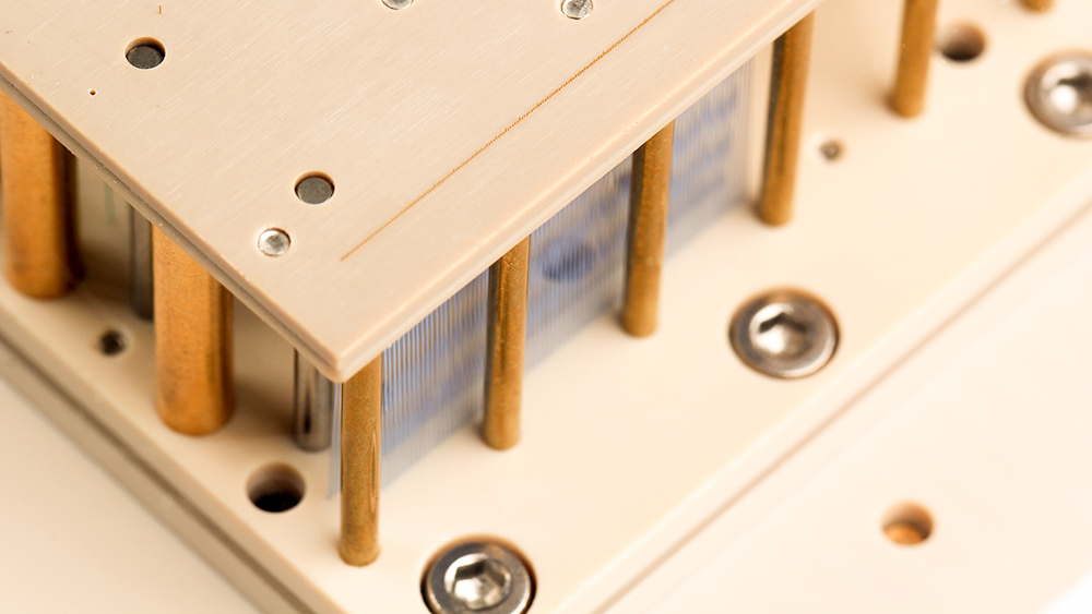
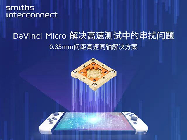
November 4, 2022 - 0900 to 1130 Shanghai/CST“同轴结构在微间距插座上的应用”
Abstract - Biography (English)
As technology advances, mobile devices have the most complex and high-speed system-on-chips (SoCs) ever produced. The request for increased functionality in the smallest possible footprint has led to a reduction of chip pitch below 500?m. High speed and fine-pitch chip testing usually uses short spring probe in test sockets or conductive elastomer sockets. But short spring probe can’t generate enough spring force for stable low Cres and conductive elastomer have limited compliance, all which impact the socket performance. Customers’ next generation device performance, require low loss signal integrity performance from test sockets for sub 500 µm pitches. Smiths Interconnect has successfully developed a coaxial structure based on patented DaVinci technology for high-speed test socket with minimum pitch to 350µm applications. It has filled up the gap of previously coaxial sockets for ?650 um pitch chip test, were only available. The coaxial structure fundamental formula means small pitch requires smaller diameter spring probe or contacts for impedance matching. The challenges to develop a production ready coaxial socket are immense. DaVinci Micro’s signal probe and IM socket housing structure have application specific configurations which have been developed and deployed to the field, which have shown excellent performance in high volume IC chip testing at our various customer sites. This paper will share the fundamental requirements of coaxial structure for micro pitch applications and our solutions for it. The basic performances including technical specifications and test results, both mechanical and electrical, will be presented to help audience understand the advantages of this technology. The challenges in the micro coaxial high speed test socket development and related solutions to meet higher speed requirement in micro pitch will also be presented.
Cleveland Chen, Bachelor of Mechanical Engineering, Nantong University; Master of Business Administration, Renmin University of China. Working in Semiconductor testing industry about 17 years; now is the Semi Eng. manager of R&D, smiths interconnect Suzhou.
摘要 - 简介 (Chinese)
随着科技的革新,移动设备里拥有繁杂且高速的系统芯片(SoCs), 在尽可能小的空间内增加功能的要求导致了芯片间距减少到500μm以下。高速且细间距的芯片测试通常使用短弹簧探针测试插座或导电橡胶插座进行测试,但是短弹簧探针无法提供足够的弹簧力来实现稳定的低接触电阻,导电橡胶的压缩行程有限, 这些都会影响测试插座性能。客户的下一代芯片测试需要500um以下间距的测试插座提供低损耗的信号完整性测试性能
Smiths Interconnect已成功开发出一种基于达芬奇专利技术的同轴结构,适用于最小间距至350um应用的高速测试插座。它填补了以前只能用于≥650um间距芯片测试的同轴插座的空白。根据同轴结构的基本公式微小间距需要更小直径的弹簧探针或者接触点来满足阻抗匹配,所以微型同轴插座在研发和生产中有巨大的挑战。Smiths Interconnect微型达芬奇信号弹簧探针和IM材料的插座已经在特定需求领域上得到的广泛的应用,并在客户量产的芯片测试中表现出色,性能稳定。
这篇文章将分享微间距应用对同轴结构的基本要求以及我们的解决方案,介绍它的技术规格, 机械和电性能。还将介绍为了满足微间距的更高速度要求,在微型同轴高速测试插座开发中的挑战和相关解决方案。
陈金荣,机械专业学士,南通大学;企业管理硕士,中国人民大学。在半导体测试行业有近十七年从业经验,现在是史密斯英特康半导体事业部(苏州)的研发部经理。
“ 基于封层结构的efuse处理代码库”
Abstract - Biography (English)
Efuse is disposable programmable memory in Semi-Conductor Chip. It will be written into specific data before delivery from factory, normally these data contain power supply voltage value, chip version, production date or trim data which reflecting characteristic of chip. During the FT/CP test, data will be written into efuse storage. Because of the disposable property of efuse storage, data which need save into efuse only have 1 time for writing action. Every single bit in efuse storage only can change status one time, this means if wrong data write into efuse memory, it can.t correct anymore! So efuse data processing is the most important part in package test for semi-conductor chip, and most of accident in package test are related to efuse data. Efuse process contains 2 parts of action: write and read, write is transfer data into chip, read is extract data from chip. Read action is often used for check write data if correct. Originally efuse test will running as below. Firstly, collecting data distribution information from chip introduction document. Secondly, developing test method for transfer real data into efuse data container. Finally, download efuse data into chip using specific protocol. Based on these steps, testing engineer will refactor test code of efuse data management. Modifying test code frequently will influence stability and robust of test program, and it will increase the risk of error occurring of test code. Many of accidents occurring in efuse test are result from this process. These accidents often lead to great financial loss for customer, and it will create huge crisis of confidence to us. For improving stability efuse test code and simplifying operation sequence of efuse test process, we develop a new efuse test solution based on Multi-Level software structure. This solution has 3 classes to manage efuse data: Die, block, node, and all updating actions for different efuse data distribution only need to editing input csv file. According to this structure, there are several features shown below:1. Less code refactoring while test program updating, it helps reducing the risk of code error occurring2. Each updating action only need to modifying specific csv file, it can reduce difficulty of operation for testing engineer3. Support Different protocol for different die in one chip and implement by D2S4. Make complicated action of remapping data distribution information with test code developing change to simple definition of node in csv file5. Extend API for support complex data processing, like encode/decode original data before/after transfer into efuse part6. Flexible code structure cause easy-migrate to different user.In a word, this solution can greatly improve using experience of efuse test developing, and compatible with different requirement. So far, we have finished most of content developing of this solution and spread to customer. Through this tool, user can reduce the probability of errors by 90% and save 60% of development time
Senior Application Engineer of ADVANTEST. Obtained a master's degree in circuit and system in 2017. Developing ATE test program more than 5 years. Engaged in digital, hi-speed, mix-signal chip testing, providing software and hardware solution of ATE Chip test for top semi-corporations in China region.
摘要 - 简介 (Chinese)
Efuse 是半导体芯片中的一块一次性可编程存储空间。它一般被用于在交付给客户前写入一些特殊的数据,一般情况下被写入的数据会有芯片工作电压,芯片版本号,量产批次,修调数据或其他一些可以反映芯片特性的数据,写入过程将会在封装或晶圆测试阶段完成。 由于efuse是一种一次性可编程的存储空间,所以一旦数据被写入该区域中,就无法被后期修改为其他信息。或者严格来说每一个字节的内容只可以被修改一次,这将意味着一旦写入数据出现错误,而这颗芯片也将直接报废。所以efuse烧写是整个半导体芯片加工制造过程中十分重要的环节,尤其是在封装测试环节十分容易由于efuse的问题而导致大量芯片的报废。Efuse工作包含两个环节:写入和读取。写入是指将有效内容通过某些协议写入到芯片中,读取是指通过某些协议将芯片efuse存储区域的内容读取出来,该动作可以用于检查写入数据是否正确。 一般情况下efuse工作流程如下:首先通过芯片手册确定efuse中不同类型数据的区位分布情况。其次,开发测试代码用于完成传输和收集需要写入的efuse数据。最后将这些需要写入的efuse数据通过指定的协议形式传输到芯片中。基于以上这些步骤,测试工程师需要频繁更新efuse数据管理相关管理相关代码。频繁修改测试代码会严重影响程序的稳定性和安全性,同时也会导致测试代码出错的概率增加。实际操作过程中许多事故都是由于测试代码修改操作导致的,并且通常这些事故都会造成十分严重的经济损失。 为例提升efuse操作环节的稳定性同时简化操作流程,我们开发以一套全新的基于多级分层结构的efuse处理解决方案。这套解决方案通过三层结构管理efuse数据,芯片级, 地址级, 结点级。并且所有更新数据的操作只需要修改对应的表格即可。通过这些结构,可以实现以下优势特点: 1.程序更新只需要很少的代码修改,这将会大大减少发生代码错误的机率 2.程序更新的操作只需要修改表格文件,这可以大大降低操作的难度 3.支持同一颗芯片不同的模块使用不同的协议写入efuse数据 4.使复杂的数据内容重构或重新映射的操作变成简单的表格操作 5.可扩展的程序接口可以用于支持复杂的efuse数据处理,比如efuse数据的编解码操作 6.灵活的代码结构可以实现更加优秀的兼容性 总之,这套efuse处理的解决方案可以很大程度上提升efuse测试代码开发的使用体验,同时还可以在不同产品间做到最大程度的兼容。目前为止,我们已经完成了所有的代码开发并且将其交付给多加客户。通过这套工具,用户可以降低efuse相关代码90%的不稳定性,同时还可以节省60%以上的开发时间。
爱德万测试高级应用开发工程师,于2017年获得电路与系统专业硕士研究生学位,有5年的ATE测试程序开发经验,主要从事数字,模拟及高速类芯片测试程序开发,长期为国内顶级半导体研发公司提供基于ATE平台的软件及硬件解决方案。
“使用 DPU-16板卡驱动两个以上的引脚电平”
Abstract - Biography (English)
When it comes to low carbon living and low power consumption in the world, it’s necessary for reducing the device size and pin count. For example, a certain kind of device would combine with a clock pin and an enable pin as only single pin to limit the pin count in some scan chain structures. Therefore, it requires to drive more than two different pin levels on the pin to generate combined signal. This paper will explore several solutions to drive more than two pin levels on one pin with DPU-16 board. First of all, it describes the background and requirements. Then it shows how to drive the third pin level with VTT mode and what’s the restriction. After that it explores other solutions, like adding additional circuit and adding two DPU channels by connecting one resistor to drive more pin levels. At last, with one suitable formatter, it can generate the expected waveform shape which can get the correct ratio of low/high pin levels with only one DPU channel.
Evan started to join Teradyne since from 2014 as an Application Engineer of SEG group. As an engineer, he focuses on the developing for test concept and test solution for all kinds of devices for customer, such as high power chips for IGBTs and MOSFETs, PMIC chips for LED drivers and DC-DC converters, etc. Evan has rich experience in a variety of ATE test equipment, and is able to flexibly use test machines such as Flex/Ultra flex plus/ETS88/ETS88-TH/ETS800.As a member of the semiconductor industry, Evan will continue to serve more customers in the future.
摘要 - 简介 (Chinese)
随着全球半导体技术的飞速发展,减少芯片的封装尺寸和冗余的芯片引脚是一种趋势。例如某种芯片会把时钟信号引脚和使能信号引脚结合到一起,作为单一的引脚,以限制某些scan链结构的芯片引脚数。因此,需要在这个单一的芯片引脚上驱动两个以上不同的引脚电平才能产生组合信号。本文将探讨几种关于如何使用 DPU-16 板卡在一个引脚上驱动两个以上不同引脚电平的解决方案。首先,描述了背景和需求。其次,介绍了DPU-16板卡的性能参数,以及展示如何使用VTT模式驱动第三个引脚电平及其限制。之后,探索了其他的解决方案,例如添加额外的电路和通过两个DPU通道之间连接电阻器来驱动更多的引脚电平。最后,通过使用合适的信号格式,它可以生成预期的波形形状,只需一个 DPU 通道即可获得正确的引脚高低电平比率。
Evan 从 2014 年开始加入泰瑞达公司,担任 SEG 组织的应用开发工程师。作为一名工程师,他专注于为客户开发各种不同芯片的测试概念和测试解决方案,如 IGBT 和 MOSFET 的大功率芯片、LED 驱动器和DC-DC 转换器的 PMIC 芯片等。Evan拥有多种ATE测试设备经验,能够熟练使用和掌握Flex/Ultra flex plus/ETS88/ETS88-TH/ETS800等多种测试机。作为半导体行业的一员,Evan 将在未来继续服务更多的客户。
“基于ETS364平台测试高精度的SAR ADC”
Abstract - Biography (English)
SAR ADC is mainly applied in battery-operated systems, industrial control and remote data acquisition. It has high resolution, high accuracy and low noise. DIB design and test solution development for 16-bit SAR ADC on ETS364 platform is a challenge. QPLU is a low noise, high stability and high precision instrument, it can be used to test DC linearity error of ADC using servo loop method on ETS364 platform. This paper will focus on how to employ ETS364 instruments and optimize DIB design to achieve good testing performance. Here are the topics we are going to cover: 1. How to select front-end filter components to optimize ADC performance. 2. How to design filter for ADC dynamic test items. 3. How to set QPLU parameters during debugging, QPLU rapid dither method based on a servo loop algorithm is fast and accurate for 16-bit SAR ADC linearity testing. 4. Provide a test method based on QPLU dither DAC to display the transition noise as well as a test solution to improve the noise. 5. How to change ADC output code format by using hardware modification to process and analyze the captured data more flexible.
Susan Su is an application engineer at Teradyne for over six years. In the first five years, she focused on the development of analog device and ADC/DAC on ETS 364 and ETS88 platforms, her work is mainly hardware design, coding, debugging and data collection.
摘要 - 简介 (Chinese)
SAR ADC主要应用于电池驱动系统、工业控制和远程数据采集。它具有高分辨率、高精度、低噪声等特点。基于ETS364平台上开发16位SAR ADC的硬件设计和测试方案开发是一个挑战。QPLU是一种基于伺服回路算法的仪器,具有低噪声、高稳定性、高精度的特点,可用于测试 ADC的线性度。本文将重点研究如何应用ETS364资源以及优化硬件设计,从而达到良好的测试性能。本文主要包括以下五个方面:1. 如何选择前端滤波器来优化ADC性能。2. 如何设计滤波器来改善ADC动态性能。3.基于伺服回路算法的QPLU快速抖动法可以快速准确的用于16位SAR ADC线性度测试,介绍了如何在调试过程中设置QPLU参数。4. 提出了一种基于QPLU抖动DAC来显示转换噪声的方法,以及如何改善转换噪声。5. 如何通过硬件电路来改变ADC输出代码格式,便于对捕获的数据进行灵活的处理和分析。
我叫Susan Su,来自泰瑞达的一名应用工程师,我在泰瑞达工作了六年。前五年都集中在ETS 364,ETS88平台的开发,主要从事模拟芯片以及ADC/DAC的测试方案开发,主要工作包括硬件设计,程序开发,测试方案的调试和数据收集。
For any questions about the event or sponsorship contact us at [javascript protected email address].
Program subject to change without notice
Event registration is free courtesy of our sponsors
Honored Sponsor

JDT Technology's focus in the vertical field of semiconductor and electronic product testing & precision manufacturing, and dedicate ourselves to be an “Intelligent Automation Integrated Solution Provider”. Our main business includes: Probe materials, ICT / FCT test fixtures, Automated Testing Equipment & Precision Machining.
Distinguished Sponsors

Smiths Interconnect is a leading provider of innovative solutions for critical semiconductor test applications. Smiths Interconnect’s test sockets and probe card solutions offer superior quality and reliability, providing customers with a competitive advantage. Our best-in-class engineering, development and technical expertise ensure support of automated, system level and development test platforms for area array, peripheral, wafer level and Package on Package (PoP) devices as well as high performance spring probe technology and cable assemblies. Our extensive product portfolio accommodates devices with finest micro pitches as well as those with very high bandwidth requirements. Off-the -shelf and custom products are proven to deliver the best solution for the customer’s specific needs.
For more information, please visit www.smithsinterconnect.cn

Teradyne (NASDAQ:TER) brings high-quality innovative products such as smart devices, life-saving medical devices and data storage systems to market faster. Its advanced test solutions for semiconductors, electronic systems, wireless devices, etc., can ensure that products perform according to design standards. Teradyne's industrial automation products include collaborative mobile robots that help manufacturers of all sizes increase productivity and reduce costs. Teradyne's revenue in 2021 will reach $3.7 billion. Today, Teradyne has approximately 6,300 employees worldwide. For more information, visit the official teradyne.com website. Teradyne® is a registered trademark of Teradyne, Inc. in the United States and other countries.