
Virtual Event - October 26-29, 2021
Event registration is free courtesy of our sponsors
TestConX has, over the course of its twenty two-year history, established itself as the preeminent event for test consumables, test cell integration, and test operations. The program scope has expanded over these years from packaged semiconductor “final” test and burn-in to encompass all practical aspects of electronics testing including validation, advanced packaging testing, system level test, module test, and beyond to finished product test.
Last year, the 6th annual TestConX China 2020 was held as a virtual live on-line event with excellent average daily attendance of over 800 and peaked with 1188 viewers online at once. (Please see the Post-Event Report for additional details.) We will once again hold TestConX China 2021 as a virtual event using the same online platform. This will provide global attendees with the opportunity to see new locally created and developed content in addition to the best from international presenters.
Don’t miss this opportunity to be part of TestConX as we connect a larger community of test professionals and to participate in this excellent event!
“向以系统为导向进行测试的构造转变--不进则退”
Abstract (English)
With the slowing of Moore's Law, advances in packaging and chiplet technology have stepped in to continue the drive towards ever higher levels of integration. What continues unabated is the increasing complexity of realized end products and systems. Electronics is becoming pervasive in and around all aspects of our lives. As a result, beyond quality, assurances of reliability, safety, and security are drawing attention in many new application domains from electric cars to smart factories. In light of these trends, current testing methodologies and practices face daunting challenges. Thorough testing of individual components and their structural interconnects can no longer guarantee the required levels of quality and reliability of the integrated system. In this talk, I will delve into aspects of the challenges now arising, discuss how testing has to shift to a system-oriented perspective, describe what that means in terms of specific enabling capabilities, and highlight recent developments in support of this paradigm shift.
摘要 (Chinese)
随着摩尔定律的放缓,封装和chiplet技术上的进步已经在推动着更高水平的集成。日益复杂的终端产品和系统有增无减。电子产品在我们生活中无处不在。也因此,除了质量之外,可靠性、安全性和安全保障等正受到来自新的应用领域的关注,从电动汽车到智慧工厂。在此趋势下,当前的测试方法和实践也面临着艰巨的挑战。对单个组件及其结构互连的测试方式已经无法再保证集成系统所需的质量和可靠性水平。在本次演讲中,我将深入探讨目前出现的挑战各个方面,讨论测试应该如何转变为面向系统的视角,描述其在这方面赋能的意义,并重点介绍下支持这种范式转变的最新进展。
MediaTek Inc.
Harry Chen holds the position of IC Testing Scientist at MediaTek Inc. In this role, he investigates advanced design and test methodologies to enhance the performance and quality of leading-edge products. He actively participates in industry forums by publishing papers, giving talks, and serving on program committees. He also supports academic research projects and trains student interns. He is the section leader for System-Level Test (SLT) in the IEEE Heterogeneous Integration Roadmap (HIR) Test Chapter. With more than 30 years in the semiconductor industry, Harry has held previous technical positions at Cadence Design Automation and Analog Devices in the USA. His EE degrees were obtained from MIT and Stanford University.
“一种新型的刮擦接触 (J 型)”
Abstract - Biography (English)
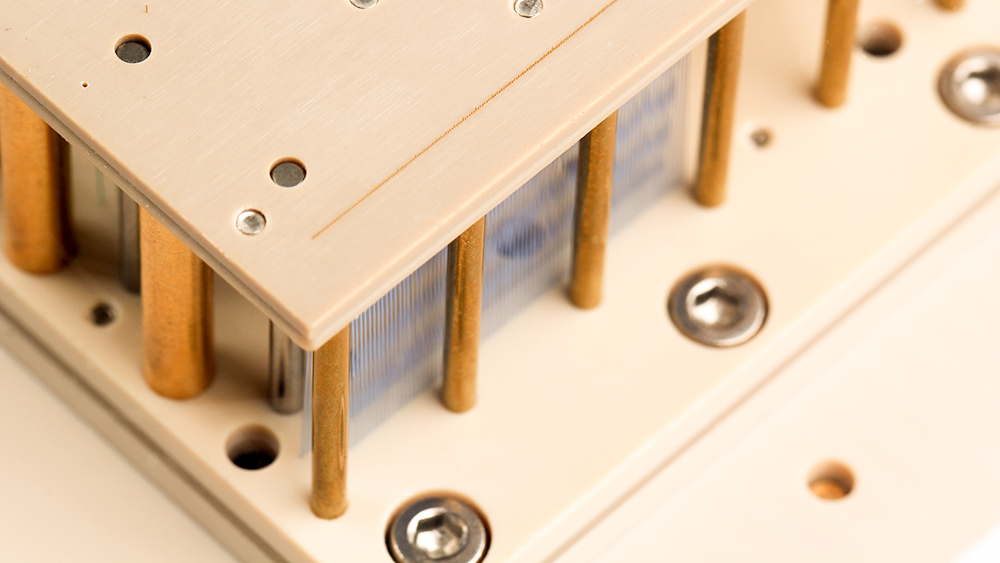
With the development of 5G and automated driving technology, the chip develops towards high-speed and miniaturization. Traditionally, there are 2 ways to test high speed IC: socket with very short spring probe and Coaxial socket; short spring probe can’t provide enough test force, the performance is unstable, Coaxial socket is expensive. So, they are not the optimal solution to test QFN, QFP, SOIC and TSPO chips.
A super short Scrubbing contact(J shaped)is developed for QFN, QFP, SOIC and TSOP chips test. It provides short signal path by optimize pin shape, by this way, it provides great signal integrity: insertion loss: 20GHz @ <-1 dB; current carrying capacity :8Amps. J shaped Scrubbing pin secures to socket using an elastomer, ensure socket can provide stable test force in large temperature range with long cycle life, low and stable resistance at small pitch.
J shaped Scrubbing pin with special shape design, from rest to test, scrubbing action ensure minimal impact on PCB pad and package pad .The GND solution in socket can provide excellent thermal performance and impedance control, It also enables longer compliance similar to a spring pin. The socket concept allow field repairable without removing socket from PCB, reduced downtime.
This paper will share the how does J shaped scrubbing pin worked, the Mechanical and Electrical properties of J shaped Scrubbing contact. What’s the challenge in J shaped Scrubbing pin test and how to meet higher speed requirement in tighter pitch?
Eric Zhang joined in Smiths Interconnect Suzhou site as a Mechanical engineer from 2010. Currently he is mainly engaged in the design, research and FEA of test sockets and lids. he graduated from Nantong University in 2006 and got a bachelor's degree.
摘要 - 简介 (Chinese)
随着5G和自动驾驶技术的发展, 芯片朝着高速和小型化发展,通常用两种方式可以测试高速芯片:使用测试长度很短的弹簧探针和同轴测试插座。这两种测试方法各有有缺点:使用短的弹簧探针插座价格便宜但是由于真太短不能提供足够的力使针尖穿破引脚氧化层,测试不稳定;同轴结构的测试插座有很好的高频性能,也能提供很好的接触力,但是价格贵,交期长。因此这两种方式都不是测试QFN, QFP, SOIC和TSPO 封装的最佳选择。
研发一种超短型刮擦测试探针(J 型)用来测试QFN, QFP, SOIC 和TSOP 封装. 它优化的外形为信号提供了超短的路径,通过这种方法很好的保证信号的完整性: insertion loss: 20GHz @ <-1 dB; current carrying capacity :8Amps. J型刮擦探针通过橡胶条固定在测试插座上,可以保证测试插座在很宽的温度范围内,保持稳定的测试力和长久的循环寿命,在小间距的情况下仍可以提供稳定的,非常低的阻值。
J型刮擦探针有特殊的外形,确保从自由状态到测试状态,刮擦动作对PCB和芯片Pad影响降到最小。测试插座的接地解决方案可以提供极佳的散热和阻抗匹配。
这篇文章将分享J型刮擦探针是如何工作的,它的机械及电性能。在高速和小间距pad中,J型刮擦探针面临的挑战是什么。
张龙自2010年加入Smiths Interconnect苏州公司设计部担任机械设计工程师,目前他主要从事于芯片测试插座的设计,研究和有限元分析。他在2006年毕业于南通大学机械设计及其自动化专业,取得学士学位。
“老化制程新技术,让你少走冤枉路”
Abstract - Biography (English)
"Production burn-in operations has multiple burn-in systems, loader/unloaders & a huge quantity of burn-in boards on racks or trolleys. With limited integration between them, significant manual handling activity had resulted in efficiency lost, board damages & resource wastages. While automation presents a potential solution in solving some of these issues, the cost of both implementation & maintenance is prohibitive, & flexibility can be significantly compromised.
This presentation relates to solving all these burn-in operational challenges, covering operator, process, maintenance, space & automation-related issues, faced by companies around the world though our patent-pending system/method.
It gives an overview of typical burn-in operation & its related issues & seeks to demonstrate how by a marginal increase in investment during capacity expansion by implementing the proposed system/method, companies can significantly improve efficiency, reduce board damage & resource wastages, even without costly automation.
The same solution is also easily upgradeable now, or in future. Let us all start to Keep It Simple & Save (KISS) money in burn-in operation."
Joe Tan is the Founder & Managing Director of MSV Systems & Services Pte Ltd established in Singapore in 2002.
He graduated from the National University of Singapore with a Degree in Electronics Engineering & Master’s in Industrial & System Engineering.
After 25 years of providing technical service on burn-in systems, loader/unloaders & burn-in boards to world leading Automotive & Memory semiconductors companies, he saw many long outstanding operational issues in burn-in.
In 2018, with the support of Enterprise Singapore, MSV developed a prototype burn-in chamber for proof of concept.
In 2020, MSV files a patent in PCT countries & Taiwan for an inventive burn-in chamber/method which will enable all companies to KISS, i.e. Keep It Simple & Save a lot of money & troubles in burn-in operations.
摘要 - 简介 (Chinese)
传统老化车间里有许多的老化系统, 装卸机,和大量的老化板。
在老化流程中,老化板在老化系统与装卸机之间不断的循环。
因为现有的设备之间有断层,所以无法实现无缝的连接。因此,在老化 车间里,我们可以看到许多的人工操作。这导致了设备与老化板子的损 坏,不仅降低了产能,也浪费了大量的时间,空间,和金钱。
目前,有些老化车间已经开始考虑自动化。但很多方案不仅造价昂贵, 灵活性低,长期维护成本也非常高,因此无法实现有效的回报率。
这演讲题目先简介老化车间的流程,并总结 30 多年来老化车间还没能 解决的 10 大问题, 包括:人工操作,流程,维护,空间使用,自动化 难处,等等。
过后再简介 MSV 的专利与技术如何能在小幅度增加增产投资预算下, 解决老化车间的 10 大问题,并在无需完全自动化的前提下,实现高 效,低维护的老化制程。
在验证了专利设备和技术的运行后,车间部分现有的老化设备也能用较 低成本,通过提升后,融入新产线,实现高效,低维护的老化制程。
希望 MSV 的专利能够让大家成就:
老化制程新技术,让你少走冤枉路。
陈德发是 MSV 公司的创始人。MSV 公司于 2002 年在新加坡成立。
他毕业于新加坡国立大学电子工程系,也是工业系统工程系的硕士。
经过多年为国际厂商维护半导体老化系统, 板子, 自动化设备的经验,他 总结了 30 多年来, 老化车间还没能解决的问题。
在 2018 年, MSV 通过新加坡企业发展局的资助,在新加坡制造科技研究 所的协助下,开始研发解决方案。并于 2020/21 年,在原型机概念验证 后, 申请了的国际专利。
他的愿景是希望 MSV 的专利能够让大家成就:
老化制程新技术,让你少走冤枉路。
“宽禁带半导体带来的“麻烦””
Abstract - Biography (English)
The massive increase in people working from home, and demand in xEVs has accelerated the adoption of wide-bandgap semiconductors in consumer and automotive products. This has introduced new testing requirements to the discrete transistor and power module focused markets. In some cases, these tests are critical to evaluating the underlying process and ensuring that a device is functional. In other cases, the test challenges are an expansion of efforts already in place with IGBTs and high voltage MOSFETs. Since these processes are new, it is worthwhile to take a closer look at these test challenges and the trends we are seeing in an effort to reach some level common understanding.
Tom Tran is a Product Manager for Power Discrete Test Products at Teradyne. With over 15 years of test development experience in power management, precision analog and mixed signal semiconductors, Tom has been instrumental to the successes of many projects on Teradyne’s ETS platform. Prior to his role as a Product Manager, Tom was a Field Product Specialist who contributed to the successful adoption of Teradyne’s power discrete testers for wafer sort and power module testing at several customer sites around the world.
摘要 - 简介 (Chinese)
随着在家办公的需求和电动车的快速增长, 宽禁带半导体产品(比如SiC,GaN)在消费和汽车电子的普及率大大加速了。这为分立和功率模组领域来了新的测试要求。一方面,这对于保障芯片的的功能尤为重要;另一方面对于IGBT和高压MOSFET的挑战也同样存在。对于这些新的工艺带来的新的挑战和趋势值得我们深入探讨。
Tom Tran是泰瑞达(Teradyne)公司的产品经理,负责功率和分立器件。Tom在功率和电源管理领域有超过15年的测试方案成功开发经验,在泰瑞达Eagle平台上有诸多成功案例。在担任产品经理之前,Tom作为现场产品专家在功率分立器件的晶圆测试和功率模组测试等领域服务于全球客户。
“从5G毫米波到6G太赫兹 :下一代射频测试的挑战在哪里? ”
Abstract - Biography (English)
As each “G” in mobile networks generations takes about eight years to follow the previous one, we’re only about five years away from facing new 6G THz test challenges. And given that 5G mobile networks are just ramping up with high volume millimeter wave devices, is it too early to start worrying about 6G test challenges? This presentation starts with an overview of the possible 6G use cases that make THz a requirement as we enter into the second half of this decade and then follows with a preview of the test challenges that can be expected for 6G beyond the current 5G millimeter wave test challenges.
Dr. Jeorge S. Hurtarte is currently Principal Marketing Technologist at Teradyne. Dr. Hurtarte has held various technical and management positions at Teradyne, LitePoint, TranSwitch, and Rockwell Semiconductors. He holds Ph.D. and B.S. degrees in electrical engineering, an M.S. in telecommunications, and an M.B.A. Dr. Hurtarte has served on the Advisory Board of Directors of the Global Semiconductor Alliance, TUV Rheinland of North America, and the NSF’s Wireless Internet Center for Advanced RF Technology. He is the secretary of the IEEE 802.11ay task group. Dr. Hurtarte is also professor at the University of California, Santa Cruz and at the University of Phoenix. He is the lead co-author of the book Understanding Fabless IC Technology.
摘要 - 简介 (Chinese)
由于移动网络每一代都需要8年左右的时间来发展,才可以追赶上一代的脚步,我们距离面对6G太赫兹的测试挑战只剩5年时间了。考虑到5G移动网络的毫米波芯片才刚刚开始起量,现在就开始讨论6G太赫兹的测试挑战是否为时过早? 这次的演讲首先会概述6G太赫兹可能的应用场景,为什么需要我们进入6G发展的下半个10年,以及6G相比于5G毫米波而言存在着哪些测试挑战。
Jeorge S. Hurtarte博士目前是泰瑞达的首席营销技术专家。Hurtarte博士曾经担任泰瑞达、莱特波特、传威和罗克威尔等半导体公司的多种技术和管理岗位。他拥有电气工程的学士和博士学位,同时拥有电子通信工程硕士和工商管理硕士学位。Hurtarte博士曾今在北美莱茵的全球半导体联盟和美国国家科学基金先进射频技术无线互联网中心顾问委员会担任顾问,同时也是IEEE 802.11ay工作组的秘书。Hurtarte博士是加州大学圣克鲁兹分校和凤凰城大学的教授,他是《Understanding Fabless IC Technology》一书的主要合著者。
“毫米波芯片量产测试挑战实解”
Abstract - Biography (English)
With the development of mmWave technology and the increasing applications’ scenarios, the diversity and complexity of millimeter wave testing requirements are also increasing. Current mass production testing of mmWave faces many challenges, and existing mainstream ATE cannot meet the needs of performance and cost. This requires a combination of standard instrumentation and mmWave discrete devices to provide customized complete test solutions for mmWave test systems – which includes over the air (OTA) designs in a standard handler. With years of accumulated industry experience in automated test and standard software platform, Gubo seeks to provide a standard test solution for mmWave mass production testing to help customers achieve a balance of performance and cost.
Since 2019, Zi Wang joined Shanghai Gubo Technology Co., Ltd. As one of the core members, he served as an application engineering manager and engaged in the promotion of automation and standardization of semiconductor testing. Under his development and leadership, Gubo has gained a rapid growth for the business of semiconductor test automation.
Prior to joining Gubo, Zi Wang started his career with NI as an application engineering lead. He has engaged with more than 10 key RF semiconductor customers and built the first set of NI mmWave test platform for top-level customers in Greater China with the full solution from laboratory to mass production.
Zi Wang holds a Master’s degree in Information and Communication Engineering from Southeast University.
摘要 - 简介 (Chinese)
随着毫米波技术发展和应用场景的不断丰富,毫米波测试需求的多样性和复杂性也在不断增加。毫米波的量产测试面临诸多挑战,已有的量产设备不能兼顾性能和成本的需要。如何结合标准仪表和毫米波分离器件,提供定制化的毫米波测试系统以及包括分选仪的空口(OTA)设计,数据分析在内的完整测试解决方案已经成为行业重要需求。孤波依托自研的专业自动化测试软件平台以及积累的行业经验,为毫米波量产测试提供标准测试方案,帮助客户实现了性能和成本的平衡。
王孜作为核心成员之一在2019年加入上海孤波科技有限公司,并担任应用工程经理,从事半导体领域测试自动化和标准化的推进工作。 在他的引领下,孤波的半导体测试自动化业务实现了快速增长。
在加入孤波之前,王孜作为系统应用工程师在 NI 开始了他的职业生涯,帮助10余家射频类半导体客户提供测试解决方案,并为顶级客户搭建NI大中华区首套毫米波测试平台,提供从实验室到量产的完整解决方案。
王孜拥有东南大学信息与通信工程硕士学位。
“应用于112Gbps Serdes测试的精确PCB仿真模型”
Abstract - Biography (English)
"With the demand of data rates up to 112Gbps in ATE testing load board design, 3D Electromagnetic simulation is widely used for signal integrity. The accurate simulation is very important for project successes. In 3D Electromagnetic simulation, the material model is the base for the simulation and dominate the result accuracy. In traditional simulation model, many assumptions are used for simulation model and the result is always discrepant when compared with the real-world measurement.
This paper analysis the inaccurate PCB simulation model using traditional PCB model. After extract material properties from prototype board, the new accurate PCB model is created, which shows good correlated with measurement result. S-parameters Measurement and cross-sections of PCB are used in this paper to identify the parameters of material properties suitable for analysis of PCB with manufacturing variations. This accurate PCB model including material properties will guarantee the Hardware performance designed by Teradyne."
Ming-Tong Zuo received the Master degree from Tongji University, Shanghai in 2018. He has worked in Teradyne for 3 years as SI/PI simulation engineer.
摘要 - 简介 (Chinese)
随着ATE测试载板上的测试频率的需求达到112Gbps,3D 电磁场仿真被广泛地应用于保证信号完整性之中。 精确的仿真对于项目成功与否至关重要。在电磁场仿真中,材料模型是仿真的基础,且决定了结果的精确度。传统的仿真模型采用了很多假设条件,而仿真结果也往往与实际测量之间有较大的偏差。
本文分析了传统PCB仿真模型的不足之处。我们从原型板上抽取出材料属性,创建了新的PCB仿真模型,该模型与实测结果达到了很好的一致性。本文通过S参数测量与PCB横截面测量来获取材料属性参数,该参数可适用于包含生产误差的PCB仿真分析。这一包含材料属性的精确仿真模型可以保证泰瑞达公司硬件设计的良好性能。
左明桐,2018年获得上海同济大学硕士学位。3年来工作于泰瑞达(上海)有限公司,从事SI/PI仿真工作。
“毫米波芯片量产OTA测试挑战”
Abstract - Biography (English)
Antenna in package(AIP) modules are manufactured in high volume due to its use in mobile phone that support 5G FR2.
These modules have no access to its mmWave transceiver other than via its antenna build into its package.
Over-the-air(OTA) testing by using the AIP’s antenna is necessary to evaluate the module’s mmWave performance.
Validation of AIP or antenna using OTA testing have been done for decades. However, implementing mmWave OTA testing in a high volume manufacturing (HVM) production is fairly current.
The current conventional semi-conductor test setup in production are inadequate for mmWave OTA testing.
Some of the unique OTA requirements such as mmWave testing requirements, special made mmWave antenna for handlers/sockets and handling of device without blocking its antenna are not available in current HVM production floor.
This presentation will introduce OTA testing and the challenges of doing it in a HVM environment.
Some general solution will be also be highlighted
Frank Goh is a principal application consultant in the wireless center of expertise for Advantest. For more than 20 years, he has been developing test applications from mmWave, RF, mix-signal to DC. For the past few years, he is working more on mmWave 5G applications and OTA testing. Frank has an Engineering degree as well as Master of Science degree from National University of Singapore.
摘要 - 简介 (Chinese)
5G的FR2 采用了毫米波频段,在这个频段,天线尺寸足够小,可以做到芯片封装中形成了AIP(Antenna in package)。目前5G手机的商用进入成熟阶段,相应的AIP模块也需要大规模量产。
在测试中,AIP模块的信号只能通过内置天线直接在空气中传播,而非射频线缆进行传输,这样的 方法称为OTA(over the air)测试。
很多年前,OTA测试方法已经被采用,用作测试和评估模块的mmWave毫米波频段的性能。但是并没有作为大规模量产的手段。目前5G毫米波频段的大量应用,以及AIP封装的成熟,使得OTA第一次要用于大规模量产级别的半导体测试和生产。对于业界,这还是全新的挑战,相关应用还在探索和成熟的过程中。
测试生产中,有很多新的要求,例如为了和AIP模块建立射频通信信道,半导体量产环境需要进行相应的特殊设计。毫米波天线需要集成到handler和sockets中去,生产中如何不干扰AIP模块和测试环境间的OTA射频通信,等等。
本文将针对这些量产环境中的OTA测试方案和全新挑战,进行介绍。并且着重对一些通用方案进行讨论。
Frank Goh 在爱德万测试公司专家中心担任Principal应用顾问。在其25年的职业生涯中, Frank致力于开发从DC到混合信号、射频、毫米波的测试方案。在最近几年中, 他主要研究毫米波及相关的OTA测试领域。Frank毕业于新加坡国立大学,获得本科和硕士学位。

VLSIresearch
Lin is a Principal Analyst of VLSI Research Europe. She received the Doctoral Degree in Engineering from University of Cambridge in 2017. Lin has published more than 20 academic papers as the first author or co-author in the IEEE Transactions, SUST, Journal of Physics D etc.
Lin started to join VLSI Research Europe from February 2017, focusing on the technical and marketing research and analysis related to semiconductor test consumables. She has been responsible for expanding VLSI Research Europe's coverage of the test consumables market, which now includes detailed breakouts of the non-memory market and market data on materials and components.
“移动磁力计终端测试 - 从取放到晶圆级测试处理”
Abstract - Biography (English)
"For years Pick-and-Place test handling solutions have been the state-of-the-art technology for MEMS sensor handling in Final Test. Today, increasingly demanding test requirements for sensors and ever shrinking device sizes, introduce more and more challenges to this approach. This talk explores how Wafer-Level Final Test solutions for suitable packages like LGA’s, QFN’s, BGA’s, Fan-Out and WL-CSP’s help to overcome these challenges and improve overall process yield and Cost of Test.
By the example of magnetometer sensors, where CSP type packages are increasingly seen in the marketplace, we explore how Wafer Level Final Test can reduce the overall number of pick-and-place steps in Final Test, reduce conversion time and tooling cost for new packages, resulting in the above-mentioned yield increase and Cost of Test reduction.
Furthermore, improved magnetic stimulus options available for Wafer Level Final Test allow a more accurate calibration of sensors, adding even more value to this innovative test approach."
Michael has more than 25 years of experience in the semiconductor industry and is currently holding a position as Director Sales and Marketing with Afore Oy, a Finland based provider of application specific test solutions for MEMS and other semiconductor devices. In this position he has high visibility on current and future requirements for test applications, especially in regards to final test and calibration of MEMS sensors.
Michael has a technical background and started his career as service and applications engineer for laser based marking and process equipment supporting first a European and then a global customer base. Prior to his appointment with Afore he held several sales and marketing positions for semiconductor equipment related to wafer metrology, device handling and reliability.
摘要 - 简介 (Chinese)
多年来,芯片取放测试方案一直被认为是目前MEMS传感器终端测试的“最先进技术“。如今,由于传感器的测试要求的提高和器件尺寸的不断缩小,这类取放式方法正面临越来越多的挑战。本演讲将探讨适合诸如:LGA’s, QFN’s, BGA’s, Fan-Out 及WL-CSP’s等封装形式晶圆级的终端测试解决方案如何能帮助克服这些挑战的,以及如何改善整体工艺产量和测试成本的。
以磁力计传感器为例,CSP型封装在市场上越来越多,我们探讨了晶圆级终端测试如何减少测试中的取放步骤总数,减少对新封装的转换时间和工具成本,从而实现了上述增加产量和降低整体的测试成本。
此外,通过经改进的磁激励选项,能使晶圆级终端测试做到更精确的传感器校准,从而为这个创新的测试方法增加了更多的价值。
Michael在半导体行业拥有超过25年的经验,目前担任Afore-Oy的销售和市场总监,Afore- Oy是芬兰的MEMS和其他半导体器件专用测试解决方案提供商。在此职位上,他对测试应用程序的当前和未来要求具有很高的知名度,尤其是在MEMS传感器的最终测试和校准方面。
Michael拥有技术背景,并从服务和应用工程师开始其职业生涯,主要是为激光打标和处理设备服务,首先为欧洲客户,然后为全球客户提供支持。在被任命为Afore之前,他曾担任过与晶圆计量,设备处理和可靠性相关的半导体设备销售和营销职位。
“ IoT芯片一站式测试解决方案 ”
Abstract - Biography (English)
With the development of technology in China, there are lots of fabless customers who devote themselves to IoT devices designs. They are sensitive with market change and flexibly change their design to meet the market need. Such IoT devices have more diversified functions, can carry more kinds of communication standards (i.e. BluetoothLE, Wi-Fi5/6/6E, NB-IoT, GNSS…) and has the advantages of low power consumption and low cost. According to these device characteristics and test requirements, there are lots of test challenges, the first one is high integration of these devices, it means they include wireless module, MCU, AD/DA and PMU modules, which need high domain coverage from ATE side. Secondly, it is low-cost testing requirement, which need lower tester cost, high test efficiency & multi-site approach. Thirdly, with the rapid growth of these devices, we need shorter period in test solution/hardware and test program development. Here we will introduce a one-stop IoT device testing solution, which includes the SOC testing platform with high performance, high flexibility and low testing cost, the convenient motherboard and daughter board hardware solution that can reduce load boards costs and improve design and manufacture TAT, as well as the graphical testing IP for test program rapid development that can cover most of mainstream communication standards. Such one-stop test solution can support IoT fabless customers to quickly bring up products into the market while reducing test costs.
Daniel Sun is a senior test expert of ADVANTEST (China). He is mainly engaged in the development and promotion of 5G and IoT devices test solutions. He has more than 15 years of working experience in the field of RF testing, and has deeply studied the market development trend of 5G sub6G / millimeter wave, Bluetooth, Wi-Fi and other RF devices and the demand for mass production test of ATE.
摘要 - 简介 (Chinese)
当前,IoT芯片的功能更加多样化,能承载更多种类的通信标准,同时又兼具有低功耗,低成本的优点。从这些芯片的特点和测试要求来看,我们看到不少测试挑战。首先是芯片的高集成度,这些IoT芯片包含了射频模块,MCU、AD/DA和PMU模块,其需要测试机台有多功能的资源来覆盖不同模块的测试需求。其次,低成本的要求需要更低成本的测试机台,更高的同测效率以及更多站点的硬件方案。再次,随着这些芯片快速的更新换代,我们也需要更高效的测试解决方案,更短的硬件/软件开发周期。这里我们将介绍一种一站式IoT芯片测试解决方案,其包括:高性能、高灵活度、低测试成本的SOC测试平台,便捷的子母板硬件系统,以及用于快速开发的图形化测试IP。该方案可以支持IoT芯片设计公司在降低测试成本的同时快速的将产品导入市场。
Daniel Sun, 爱德万测试(中国)管理有限公司高级测试专家, 主要从事5G和IoT芯片测试解决方案的开发和推广。在射频测试领域有超过15年的工作经验,深入研究5G Sub6G/毫米波,蓝牙,Wi-Fi 等射频芯片的市场发展趋势和ATE量产测试需求。
“藉由雲端機器人實現SI/PI探測”
Abstract - Biography (English)
The Robotics Probing System (RPS) is an innovative zero human touch/touchless semi automatic probing system (IoT, Robotics and Augmented Reality) that aims to provide engineers to virutally control movement of oscilloscopes probes to obtain signal integrity and waveform measurement.
This solution allows remote access to preform validation and integrity test on platform that lack on availability in their geo-site with 24/7 availability.
Angie Ng See Tien is a Principal Engineer in Intel Internet of Things Group. She comes with 24 years experiences, covers R&D Electronics Design, FPGA characterization, Electrical Validation , Functional Safety, Customer Design In and Debug. Angie just obtained her Doctorate Degree in Multimedia Technology from University Science Malaysia and she is also awarded Distinguished Invention Award by Intel Patent Committee. Angie has > 10 external publications or journals as well as she is a certified PMP and ISO26262 Automotive Functional Safety Engineer. During leisure time, she practice meditation and enjoy gardening.
As a child, Lau Tuck Sheng like to figure out the intricacies of how things work, and this has translated to his passion for Engineering.
Lau graduated with a Diploma in Mechatronic Engineering in a local Polytechnic for his love of inventing with his hands. With his thirst for knowledge for modern technology in engineering, Lau then study Bachelor of Electrical Engineering Technology in the Malaysia University of Technology Malacca majoring in Industrial Automation & Robotics in 2015
Remote Cloud Debug Graduate Trainee
During his studies, he worked as a Freelance Tech-consultant in designing and developing many projects which included designing and developing a Rescue Drone for natural disaster victims, Automated Solar panel follower and Fall Detection Shoe for Elders. Coached by his father, Lau also involved himself in Tennis as a child. His interest in learning tennis was rewarded by being chosen as an athlete for the states and later on represents his university for inter-varsity games.
He is currently pursuing a Master of Engineering in University Technology Malaysia majoring in Computer &
As someone who loves to engage with robotics and automation, Mohammad Saifullah, Mohd Salman begin his automation journey begin since he was form 2 (14 years old) with Robotic Competition
Saiful graduated with Bachelor of Engineering Electrical & Electronics from Universiti Teknologi PETRONAS majoring in Instrumentation & Control. In pursuing the passion of automation, he developed a full-end Smart Parking Guidance System and published IEEE paper for the project during his final year. The project won Silver Award for best Final Year Project that hosted by IEEE Control & Automation. He able to linked what he learnt in university with industry when he did his internship at Intel Penang 2016. With the thought of contributing to nature, he developed reward-based recycle bin where anyone who throw the trash according to the bin colours will be rewarded. This invention won second place in Science Engineering Design & Exhibition (SEDEX).
A strong believer automation is not only about brainstorming, it does required creativity to tackle the problem. Thus, he started his journey on photography to develop that particular side of creativity and won few awards at international level for his amazing shot.
Currently, he is pursing a Master of Engineering Electrical & Electronic (Research Mode) at Universiti Teknologi PETRONAS majoring in Instrumentation & Control (AI-Data Related).
简介 (Chinese)
Angie Ng See Tien 是Intel物聯網事業部的首席工程師。她擁有 24 年的經驗,涵蓋研發 電子設計、FPGA 特性、電氣驗證、功能安全、客戶設計和除錯。Angie剛從馬來西亞科 學大學獲得多媒體技術博士學位,她還獲得了Intel專利委員會頒發的傑出發明獎 。Angie 擁有超過 10 篇的對外發表或期刊,並且她還是一名經過認證的 PMP 和 ISO26262 汽車功能安全工程師。在閒暇時間,她練習冥想並喜歡園藝。
“深度学习在Shmoo数据结果分析中的应用”
Abstract - Biography (English)
Shmoo plot is a common method in the field of semiconductor testing to verify whether the specification of product can meet target or not. Shmoo plot analysis is also an important way to help test engineer to debug testing vector/pattern to find out the potential problem in chip design. What is more, the result of Shmoo plot analysis can benefit the yield ratio. This method always exams the characterization from the aspect of supply voltage and operating frequency. However, the review work of Shmoo plot result is managed manually, especially in the process of ATE test. As the chip become more and more complex, the amount of Shmoo plot in a single project become so large that much more time is spent on this part, hence extend the testing period, which impact the time to market. In this paper, a Shmoo result analysis tool based on deep learning is introduced, which can help to analyze the Shmoo result automatically in a short time with high test accuracy. This tool is developed under Python and PyTorch. My efficient tool is designed based on AlexNet with modification which adapt to the characteristics of Shmoo. These modifications can be benefit to the test accuracy eventually. In addition to the realization of the basic good and bad (Pass/Fail) second-class judgment, four labels have been added: Hole, Voltage Wall, Frequency Wall and Marginal to indicate the specific results of Shmoo.
Chao Zhou is a field application engineer in Teradyne Shanghai. He has been 8 years in Teradyne with major activity in SOC testing solution development and data analysis.
摘要 - 简介 (Chinese)
Shmoo是半导体ATE测试领域常用的一种验证产品的规格是否符合目标的方法。Shmoo分析也同样是帮助测试工程师调试测试向量,以找出芯片设计中的潜在问题的重要方法。这种方法总是从电源电压和工作频率方面进行特征分析。利用Shmoo来分析结果的最终目的是帮助提高成品良率。然而,特别是在ATE测试过程中,对Shmoo结果的分析工作往往都是手动完成的。随着芯片变得越来越复杂,单个项目中的Shmoo图量变得非常巨大,以至于更多的时间需要花在这部分,拖长了测试周期,影响了上市时间。本文介绍了一个基于深度学习的Shmoo结果分析工具,它可以帮助在短时间内自动分析Shmoo结果,并具有较高的测试精度。这个工具是基于PyTorch开发的,神经网络的结构是基于AlexNet设计的,并根据Shmoo的特点进行了优化。这些修改最终会有助于提高分析预测的准确性。除了实现基本的好和坏(Pass/Fail)的二类判断外,还增加了四个标签:Hole、Voltage Wall、Frequency Wall和Marginal,表示Shmoo的具体结果。
周超
- 现场应用工程师,泰瑞达(上海)有限公司
- 在泰瑞达工作了8年,主要从事SOC芯片测试方案的开发调试和数据分析的工作
“测试方案开发的质量和效率保证 —在ATE行业中搭建软件生态系统 ”
Abstract - Biography (English)
ATE systems and SOC solutions are becoming increasingly complex, and the rapidly increasing complexity is putting new pressure on production test solution and test program development. To accomplish shorter design cycles for fast time-to-market, and higher quality assurance approaching zero-defect to end-customer, this paper will present some solutions to address the comprehensive test development challenges, by building the integrated software ecosystem. The ecosystem aimed in reducing development time and improving test program quality during the whole life cycle of test program development. It supports test program co-development by multiple engineers, test program auto generation, test performance optimization, debugging efficiency enhancement, etc. In a summary, it is a high productivity software system with excellent expansibility, compatibility, and adaptability.
Over the past 7 years Jackie Xu has been committed to the software development related to semiconductor testing, especially for Teradyne UltraFlex. UltraFlexplus and J750 platforms supporting, he has extensive development experience dealing with semiconductor test program analysis, test program automation and quality and efficiency improvement. Has published on TUGx on how to develop tools to automatically generate test programs and given presentations in Europe, South Asia and Shanghai events.
摘要 - 简介 (Chinese)
在当前的ATE行业,ATE的系统和SOC解决方案已经变得越来越复杂,复杂度的迅速增加对测试方案和测试技术产生新的压力。为了赢得更大的市场份额,我们需要能够给客户提供更好,更快的服务,帮助客户缩短设计和开发周期,减少缺陷并提高测试质量。
软件生态系统的概念是一个能够提高生产效率的软件系统,它应该具有良好的扩展性、兼容性和适应性,目的是在测试程序整个生命周期内减少开发所需时间并提高测试程序的质量。软件生态中会包括一系列彼此相互关联或者支持的软件,比如支持测试程序的联合开发工具,能够自动生成测试程序的工具,检测并优化测试性能的工具,分析测试结果并形成报告的工具等等。
7年的工作中,一致致力于半导体测试相关的软件开发,特别是对于泰瑞达UltraFlex, UltraFlexplus以及J750平台的软件支持有着丰富的开发经验。擅长处理半导体测试程序分析,测试程序自动化以及质量和效率提升方面。曾在TUGx上发表关于如何开发自动生成测试程序的文章,并于欧洲,南亚及上海发表演讲。
“可扩展ATE平台上的一体化BMS芯片测试”
Abstract - Biography (English)
EV works with power battery. And power batteries must be monitored, that is battery monitor system (BMS). The responsibilities of BMS include battery capacity, charge and discharge control, real-time monitoring of battery safety status, and so on.
Now, people have the increase in the endurance requirements of EV cars, combined with the iteration of fast charging technology. That means the trend of BMS devices will be a single chip that can monitor much more series-connected battery packs, with higher voltage accuracy monitoring requirements. At the same time, BMS should response quickly during cells balancing. For example, the x16-cells analog front-end (AFE) chip should be tested on 80V range, and x24 AFE should be tested on 120V range. Each cell needs a monitoring pin that means standalone test channels should be arranged to each pin to simulate battery cell status. For more accurate monitoring of batteries status, the high precision ADCs what are the core units in AFE has more than 12-bits, and LSB may be less than 100uV. In terms of battery balancing, much more AFE integrated balancing MOSFET. So Rdson should be tested when high voltage is forced. In general, this requires a transient current of several amperes.
This paper will focus on how to achieve high voltage excitation, high accuracy ADC measure, and transient high current measurement in single test flow.
Kun Xu, a business development expert of Advantest (China), focuses on automotive electronics market research, testing solution design of automotive chips, etc. He familiars with various related testing processes including AEC-Q100. Kun Xu has more than 15 years of experience in semiconductor device testing, takes many test solution development and implementation, such as MCU, application processor, baseband, complex PMIC, RF devices, and so on.
摘要 - 简介 (Chinese)
新能源汽车离不开动力电池,而动力电池离不开电池监控系统BMS。电池的电量监控、充放电控制、电池安全状态的实时监控,都是BMS芯片的工作职责。 随着大众对新能源车续航要求的提升、快充技术的迭代等,BMS芯片的发展趋势将是单颗芯片可以监控更多的串联电池组,监控电压精度要求更高,监控间隔时间更短,电池平衡反应更快。这些新的技术趋势对BMS芯片的测试也提出了更高的要求。例如,16节串联BMS中,模拟前端芯片要求80V的测试条件, 24节BMS则需要120V测试条件;每个电芯节点都有监控引脚,需要独立测试通道加载可调节电压,用来模拟电池状态。为了更加精准的监视电池的状态,作为模拟前端核心的高精度ADC,其位数超过12bit,LSB可达100uV以下。在电池平衡方面,越来越多的BMS模拟前端芯片集成了放电MOS管,所以需要在大电压测试MOS管的Rdson。而这通常需要几个安培的瞬态电流。 本文将聚焦于如何在一个测试流程中,实现高压激励、高精度直流量测、瞬态大电流测试等要求。
徐琨,爱德万测试(中国)管理有限公司业务发展专家,专注于汽车电子的市场调研、汽车电子芯片测试方案设计等。熟悉包括AEC-Q100在内的多种汽车芯片测试流程。在半导体芯片测试领域从业超过15年,涉及包括微控制器MCU、应用处理器、基带处理、复杂电源管理PMIC、射频类等各种芯片的测试方案开发与实现。
For any questions about the event or sponsorship contact us at [javascript protected email address].
Program subject to change without notice
Event registration is free courtesy of our sponsors
Honored Sponsor

JDT Technology's focus in the vertical field of semiconductor and electronic product testing & precision manufacturing, and dedicate ourselves to be an “Intelligent Automation Integrated Solution Provider”. Our main business includes: Probe materials, ICT / FCT test fixtures, Automated Testing Equipment & Precision Machining.
Distinguished Sponsors

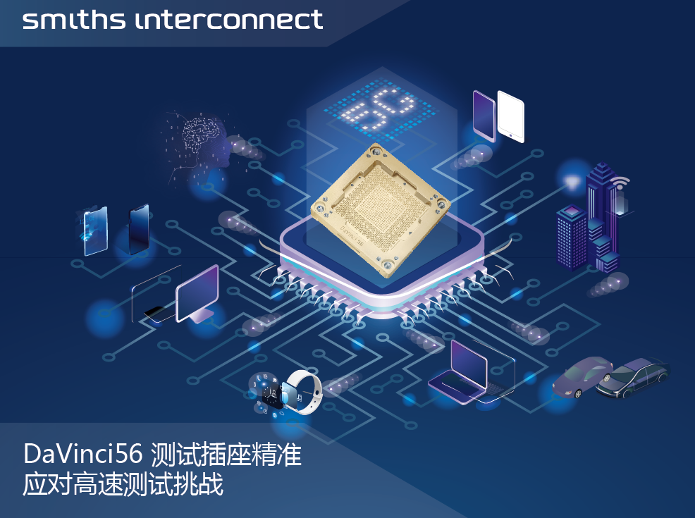
Smiths Interconnect is a leading provider of innovative solutions for critical semiconductor test applications. Smiths Interconnect’s test sockets and probe card solutions offer superior quality and reliability, providing customers with a competitive advantage. Our best-in-class engineering, development and technical expertise ensure support of automated, system level and development test platforms for area array, peripheral, wafer level and Package on Package (PoP) devices as well as high performance spring probe technology and cable assemblies. Our extensive product portfolio accommodates devices with finest micro pitches as well as those with very high bandwidth requirements. Off-the -shelf and custom products are proven to deliver the best solution for the customer’s specific needs.
For more information, please visit www.smithsinterconnect.cn


"Toward the Company Creating the Future Value of Technology"
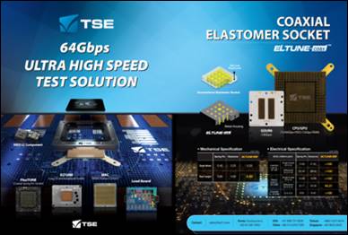
As a Technology and Science Enabler in the field of Semiconductor Test and Display Test, TSE has developed the innovative technologies needed by its customers and has engaged in continuous research and productivity improvement activities. Founded in 1994, it has engaged as a leader in interface systems for Semiconductor Test.
Exhibitor Sponsors
Advantest is the leading manufacturer of automatic test and measurement equipment used in the design and production of semiconductors for applications including 5G communications, the Internet of Things (IoT), autonomous vehicles, artificial intelligence (AI), machine learning, smart medical devices and more. Its leading-edge systems and products are integrated into the most advanced semiconductor production lines in the world. The company also conducts R&D to address emerging testing challenges, produces multi-vision metrology scanning electron microscopes essential to photomask manufacturing, and offers groundbreaking 3D imaging and analysis tools. Founded in Tokyo in 1954, Advantest is a global company with facilities around the world and an international commitment to sustainable practices and social responsibility.