|
March
7-10, 2010 |
Burn-in & Test
Socket WorkshopTM |
|
|
|
BiTS Home
Archive
Committee
Subscribe
Links |
|
BiTS
is the world's premier workshop dedicated to
providing a forum for the latest information
about burn-in and test socketing, and related
fields.
At BiTS you'll find a comprehensive technical
program, exhibits of the latest products and
services, and many opportunities to meet,
network and explore ideas with other test and
burn-in socketing professionals.
Click here if you need the latest Acrobat(R) reader
from Adobe(R):

or
for an alternate free PDF
viewer, download the latest
Sumatra PDF
It is FAST! |
|
|
|
|
COPYRIGHT NOTICE |
|
The papers in this publication
comprise the proceedings of the 2010 BiTS Workshop. They reflect the authors’
opinions and are reproduced here as presented
with occasional minor edits. Their inclusion in
this publication does not constitute an endorsement by the BiTS Workshop, the
sponsors, BiTS Workshop LLC, or the authors.
There is NO copyright protection claimed by this publication; some tutorials may
be copyrighted.
However, each presentation is the work of the authors and their respective
companies: as such, it is strongly suggested that any use reflect proper
acknowledgement to the appropriate source. Any questions regarding the use of
any materials presented should be directed to the author/s or their companies.
All photographs on this page are copyrighted by BiTS Workshop LLC. The BiTS logo
and ‘Burn-in & Test Socket Workshop’ are trademarks of BiTS Workshop LLC.
|
|
|
|
|
Technical Program |
|
Authors from around the world shared their
latest work in 30 Papers and Posters covering a prominent
range of timely and fundamental topics.
A TechTalk session
was introduced, where Tom Bresnan and Guy Ramsey of R&D Circuits shared
their deep knowledge of PCB design and fabrication for printed circuit board products
specializing in ATE.
Gert Hohenwarter of Gatewave Northern, the Tutorial instructor, went in depth on
basic RF theory and testing tools and techniques used to characterize
high speed electrical parameters of sockets and interconnects.
Françoise von Trapp, editorial director of 3D InCites and
self-proclaimed 'Queen of 3D' reviewed the latest trends and technologies
related to 3D packaging challenges gave a brief overview of the 3D roadmap, and
highlighted the
technology benefits of 3D TSV adoption in her Invited
Speaker address. This set the stage for her main challenge on test’s
readiness for 3D TSV.
Keynote Speaker, Ken Butler, of
Texas
Instruments, updated the attendees on the latest developments in adaptive test,
while Distinguished Speaker Tom Di Stefano of
Centipede Systems gave a peek into the manufacturing possibilities of
testing packaged parts in trays.
Finally, Brandon Prior of Prismark Partners
returned to BiTS to give attendees an update on the latest in low cost / small
form factor packaging and
interconnect trends in his Market Update talk.
|
|
BiTS EXPO
2010 |
|
41 exhibitors, from
socketing and related industries, exhibited their products and services
during breaks in the technical program. Click
HERE for more
info on BiTS EXPO 2010. |
|
Participants |
|
BiTS 2010 brought together well over 300 participants,
including nearly 250 full conference attendees, and 41 exhibitors from
around the world, representing end users and suppliers of sockets, boards,
burn-in systems, handlers, packages and other related equipment, materials and
services. |
|
BiTS 2010 in the Press |
|
|
|
BiTS
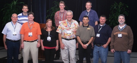
2010 Organizing Committee |
| Front: Paul Boyce (Advantage Specialist), Owen
Prillaman (Tech-Connect Sales), Kena Pegram (Sanyu Electric), Fred Taber
(BiTS Workshop), Chris Garza (Conference Management Services), Mark
Murdza (Cascade Microtech), John Moore (Texas Instruments)
Back: Valts Treibergs (Multitest), Joachin Moerbt
(Advantest Europe), Steve Hamren (Micron)
Not pictured: Marc Knox (IBM), Rafiq Hussain
(AMD), Tim Swettlen (Intel), Morton Jensen (Intel), Ila Pal (Ironwood
Electronics) |
 |
|
|
|
TechTalk |
PCB
Design, Fabrication and Assembly |
2010techtalk.pdf
 (3.26 MB)
|
|
 |
Tom Bresnan
Sales Manager |
|
 |
Guy Ramsey
Assembly Division General Manager |
|
R&D Circuits |
|
|
TechTalk covers producing the printed
circuits boards you want - from start (Design) to (Fabrication) finish
(Assembly)”.
With escalating electrical performance demands, the Printed
Circuit Board is not only an essential part of a package test and/or burn-in
solution, but has become an integral component for success. This TechTalk offers
attendees an interactive, across the board examination of those PCBs sitting
under your socket. The focus is on learning about the challenges to
properly select materials, layout, manufacture and assemble the PCB. In
‘bringing the Printed Circuit Board shop to the ‘classroom’, a better
understanding of the challenges you and your PCB vendors face is discussed.
First a brief history of the PCB or PWB (Printed
Circuit/Wiring Board) industry is covered, specifically in relation to the
ATE industry. Next the talk will address the common challenges the industry
deals with in the layout of a high yielding, yet lower volume process flow. Once
designed, the discussion covers the main cost and technical drivers of the
PCB. Those being the pitch, layer count, board thickness and via drill hole
diameter (to name but a few of the critical attributes of today’s interface
boards). Once built, the presentation explains the assembly challenges and
tricks that are required to complete the final PCB assembly.
Last, but certainly not least, the quality and performance
characteristics you can demand of your supplier(s) is analyzed. Even with
today’s boards becoming more crowded (with components) and pitch and pin counts
driving attributes ever smaller, there are ways to verify and validate the
quality of your interface boards with your suppliers. Attendees learn how,
with samples of data gathered over years of process development,
characterization and verification. |
| Mr. Tom Bresnan is the National Sales
Manager at R&D Circuits of South Plainfield, NJ. His more than 25 years of
Printed Circuit Board manufacturing experience includes positions in various
Engineering and Management roles for some of the world’s largest
manufacturers of complex Printed Circuit Boards, including Hadco, Multek and
Sanmina-SCI. He is a distinguished lifetime member of the IPC (a US based,
global trade organization representing the printed circuit industry)
Technical Activities Executive Committee, and has presented and published
numerous technical articles for the industry on MCM-L’s and advanced plating
capabilities. He resides in Colonia, NJ with his wife Joanne and sons, TJ
and Kyle. |
| Guy Ramsey is R&D
Circuits’ Assembly Division General Manager operating the Allentown
Pennsylvania facility. He maintains IPC Master Certification
credentials. The IPC has recognized him for distinguished committee
service in development of many Industry Consensus Standards. Areas of
special interest include statistical process control and methods for
establishing benchmarks in assembly process performance. Diverse
companies have sought his council on subjects ranging from Design for
Manufacturing and Assembly to End of Product Life Evaluation. Outside
the office, Guy serves as Vice President of the Macungie Borough Council
(elected municipal official), fiddles with antique audio equipment,
designs high performance speaker systems and toils endlessly on the 150
year old family home. |
|
|
|
Tutorial |
“SOCKET RF CHARACTERIZATION LAB” |
2010tutorial_hohenwarter.pdf
(1.27 MB)
|
|
 |
|
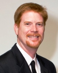
Gert Hohenwarter, Ph.D.
President Gatewave
Northern, Inc. |
Gert Hohenwarter has a Diplom - Ingenieur
degree in Elektrotechnik from the Technical University Braunschweig, Germany
and a MSEE and Ph.D. from the University of Wisconsin, Madison.
As the principal of GateWave Northern, Dr. Hohenwarter has
gained substantial experience in characterizing test sockets and probe cards
for the ATE industry. His development of high speed interfaces via
electrical, thermal and structural finite element modeling has been
instrumental in prototyping and production environments. Gert’s work also
exposes him to signal integrity prediction and verification of high speed
connectors and PCBs as well as troubleshooting on the test floor.
Gert holds several patents in the areas of high speed
connections and interfaces and is a member of the scientific research
society Sigma Xi.
|
| This
Tutorial is taught by Gert Hohenwarter of GateWave Northern, an
industry expert on socket and interconnect characterization. In this
tutorial he brings the electrical measurements lab to the
classroom.
The material and demonstrations are tailored
for both the manufacturers of test sockets as well as the end user.
The lab starts with a brief foundation of the relevant
parameters and their importance in the final application. This will
promote understanding of the basic concepts for electrical and
non-electrical engineers alike.
With that knowledge gained, various testing
configurations are discussed. Among those are traditional spring
probe test arrangements as well as more complex BGA pin arrays. Pin
pairs, differential and multi-port measurements will also be
examined. Configuration specific issues such as parasitic inductance
and capacitance of interfaces to the socket that affect socket
application as well as testing are included in this discussion.
The lab then covers various testing equipment
used in the industry including inductance analyzers, time domain reflectometers and vector network analyzers. An accounting of each
instrument’s specific strengths, weaknesses and practical
limitations is given.
A hands-on test section with scale models
operating at low frequency for ease of use allows for
examination of specific configurations during the lab.
Finally, attendees have the chance to analyze
test reports and learn how to extract the most information for their
specific application.
|
Who should have attended this
tutorial?:
This tutorial offers a great learning environment for a wide range
of workshop attendees. Those with a basic knowledge of the socket’s
electrical attributes will have the opportunity to step through all
the measurement methods and gain an understanding of how the
industry uses these results. Attendees already comfortable with
these basic concepts found both the practical demonstrations as
well as the small classroom setting with an expert helpful to
strengthening their electrical knowledge. Where else can you have
1:1 experience with an 18 year veteran in the field of signal
integrity? |
|
|
|
|
Invited
Speaker |
Rising
to the 3D TSV Test Challenge: Will You Be Ready? |
2010invited_vontrapp.pdf
(703 KB)
|
|
 |
|
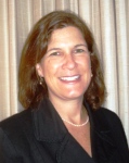
Françoise von Trapp
Editorial Director
3D InCites |
|
|
|
3D integration is not a novel concept. Veterans in the industry
will tell you it’s been around for 20 years. In fact many 3D integration
configurations, such as package-on-package (PoP) configurations, stacked die
interconnected with wirebond or flip chip, and other 3D wafer-level packaging (WLP)
technologies that utilize the existing WLP supply chain such as fan-out WLP,
Freescale’s redistributed chip package (RCP), and Infineon’s eWLB, are already
being manufactured in volume. While these configurations have most assuredly
posed challenges to the test community, the technology proving to be most
elusive is naturally the newest kid on the block: 3D ICs stacked using through
silicon via (TSV) interconnects.
However, while test solutions are high on the list of
limitations yet to be overcome, experts agree that such deficiencies won’t slow
down market adoption of 3D TSVs, and that when the time comes, solutions will be
available. Indeed, one giant step towards assuring this is communication between
the manufacturing and test communities, and in turn, an increased awareness in
the test community of what the challenges are, and what issues they’ll be asked
to solve.
As such, this talk offers a brief overview of the 3D
roadmap, the technology benefits of 3D TSV adoption, the test obstacles TSV
stacking presents, R&D efforts addressing these solutions thus far, alternatives
being suggested, and other information to help you decide if your company should
take up the gauntlet.
Ms. von Trapp is the co-founder and editorial director of 3D
InCites, a sponsor-supported, interactive online community created to stir up
interest in 3D integration. Dubbed "Queen of 3D" because of her editorial focus
on the emerging 3D integration technologies, she initially launched her blog,
Françoise in 3D, earlier in 2009. It now resides on 3D InCites. Formerly
managing editor of Advanced Packaging magazine, she became well known in the
advanced packaging community as an industry commentator, covering symposiums and
conferences, participating in trade shows, and moderating panel discussions.
Additionally, she worked with engineers, analysts, and industry executives to
develop content for both online and print publications. She holds a BA in
Communications from the University of New Hampshire, Durham NH.
|
|
|
BiTS
2010 TECHNICAL PROGRAM - SESSIONS |
| Opening
Remarks |
|
2010welcome.pdf
(562 KB)
|
| Welcoming remarks from the General
Chair, Fred Taber |
|
BiTS 2010 Keynote
Address
|
Realizing
the Benefits of Adaptive Test |
2010keynote_butler.pdf
(517 KB)
|
|
 |
|
Ken Butler
Fellow
Texas Instruments |
|
| Like most of the rest of the world, the electronics
industry is under extreme pressure to drive out cost wherever
possible. Outsourcing has become a way of life. IDMs in the US are
nearly extinct since development and manufacturing costs must be
amortized over a much larger product base. The ATE industry is a
shadow of its former self and everyone is looking for the least
expensive platform possible. It’s harder and harder to stay in
business, let alone stay competitive.
We hear a lot lately about adaptive test and the potential to use
it to reduce manufacturing costs, but what is it really? Will
adaptive test techniques make burn-in obsolete? How do we use these
ideas effectively within my manufacturing flow? How hard is it to
integrate into our existing test and data infrastructure? In this
talk we will look at the history and evolution of adaptive test. The
concepts have been around for 10 years or more, but most are far
from being considered entrenched. By comparison, on-chip scan
compression techniques were introduced around 2002 and saw pervasive
adoption across much of the industry almost overnight, at least for
large system on chip designs. Why the difference? Can the case be
made for the economic benefits of adaptive test? Of course adaptive
test is no panacea, but we will see that when it is implemented
correctly, it can do much to streamline a manufacturing operation,
speed product ramps, and reduce costs. It will require an increased
level of standardization, much improved data mining and statistical
analysis techniques, and stronger and more open communication across
the entire supply chain. But everyone who participates in the
process will benefit.
Kenneth M. (Ken) Butler is a TI Fellow in the
Design Reliability group within the External Development and
Manufacturing Division at Texas Instruments. Prior to that, he spent
13 years in TI’s ASIC Division as a design for test engineer. Ken
has a BS from Oklahoma State University and an MS and PhD from the
University of Texas at Austin, all in Electrical Engineering. He is
a Golden Core member of the IEEE Computer Society and a Fellow of
the IEEE. |
|
|
Session 1 |
Socket
Design, You Want What? |
2010s1.pdf
(1.78 MB)
|
|
We all know the story, better, faster, cheaper. But with the ever present
demand for higher speeds, finer pitches and custom packages how are we to
keep up while keeping costs under control? This session’s authors share some
ideas that address these issues. Volume manufactured, high speed test
sockets, and modular designs to manage costs and address custom package
requirements will all be on the agenda for this exciting session. |
| "Development of
a 33Ghz Final Test Socket" |
Fred Megna
MJC Electronics Corp. |
Hidekazu
"Hide" Miura
MJC Electronics Corp. |
|
| "Socket Designs
That Save Money" |
Larry Furman
Plastronics Socket Company |
Mike Ramsey
Plastronics Socket Company |
|
| "Challenges of
Test on Balls at Burn-in" |
Roland Muwanga
Intel Corporation |
Bimal Shah
Intel Corporation |
Todd Coons
Intel Corporation |
| "An Adaptable
Test Socket Concept that Meets Both the Test and Burn-In Needs of
21st Century Array Packages" |
Alexander
Barr
3M Company |
Akihiko
Furuta
Sumitomo 3M Ltd. |
Masahiko
Kobayashi
Sumitomo 3M Ltd. |
Yoshihisa
Kawate
Sumitomo 3M Ltd. |
|
|
|
BiTS 2010 Distinguished Speaker |
Test-in-Tray Perspective |
2010invited_distefano.pdf
(1.54 MB)
|
|
 |
|
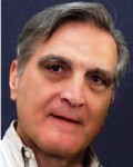
Dr. Thomas Di Stefano
President
Centipede Systems, Inc. |
|
Advances in Test-in-Tray technology have potential to
improve greatly the productivity of burn-in and test for semiconductor
electronics. With the growing complexity of IC devices, back end test
operations consume an ever increasing portion of manufacturing cost.
This trend cannot continue. Test-in-tray (TnT) enables full “lights-out”
automation through all back-end processes where individual parts are not
handled, manually or robotically, until pack and ship. The major wafer
fabs have implemented full lights out automation years ago using the
FOUP as a standard wafer carrier. A standard tray carrier serves the
same role for back end processes. Automation equipment can be
standardized around TnT for efficiency and a minimum of custom fixturing.
A recently announced FlexFrame carrier overcomes
problems that have hindered testing in tray or strip format. Although
strip testing greatly increases test throughput where applicable, the
method is limited to certain specific devices that can be tested in
strip format. Further, dimensional stability, part placement, and cost
of complex strip handlers have stunted adoption. The FlexFrame carrier
overcomes these problems by holding devices in a dimensionally stable
tray that is CTE matched to its mating contactor socket. Now, the
placement and number of devices in the tray may be matched to ATE test
capacity. The FlexFrame carrier allows easy alignment and
insertion/extraction from the mating contactor socket, greatly
simplifying the process and reducing the cost of automation.
Test-in-Tray methods are applicable to a full range of
semiconductor devices from WLP and TSV chips to complex BGA packages and
MEMS sensors. TnT has the full potential to revolutionize the test
industry – and the change is needed now. Open standards are essential to
support a great opportunity for all.
Dr. Tom Di Stefano is President and CEO of Centipede
Systems, an emerging leader in micro connection for semiconductor
electronics. Prior to founding Centipede, Tom was the founding President
of Tessera Technologies, a world leader in miniaturized packaging.
Royalties from Patents co-authored by Di Stefano generated more than
$1Billion revenue for Tessera. Previously, Tom was a Senior Manager at
the IBM T. J. Watson Research Center, where he was elected to the IBM
Academy of Technology and a member of the IBM Technology Leadership
Council. Tom earned a PhD in Applied Physics from Stanford University.
He received a BSEE Summa cum Laude from Lehigh University. Tom is an
author of more than 230 US Patents.
|
|
Poster Session |
|
2010poster.pdf
(1.34 MB)
|
|
Poster Sessions offer an additional means for scientific
communications between authors and attendees. With their interactive nature,
Poster Sessions provide authors and attendees with the opportunity to share
and explore ideas more deeply, yet less formally, than a podium
presentation. |
"New Polyarylketone
Polymer for Use in the Manufacturing
of Test Sockets: OXPEKK®"
 |
Tim Spahr
Oxford Performance Materials |
|
|
| "Shortest
Spring Pin (so far) - Practical Implication" |
Jay Kim
Western Specialty Tech, LLC |
M. G. Seo
OKins Electronics, Co. Ltd. |
|
| "POP Solution
Configurations and Challenges" |
Jim Spooner
Interconnect Devices Inc. |
|
|
| "Hybrid BK
Elastomer Socket" |
Behrouz Sadrabadi
Qualmax America Inc. |
Rani Awale
Qualmax America Inc. |
Byung-Gi Kim
Leeno Industrial Inc. |
|
“BGA Spring Probe for Final Test” |
Eichi Osato
Micronics Japan Co., Ltd. |
Fred Megna
MJC Electronics Corp. |
|
|
|
Market Update
|
Low
Cost, Small Form Factor Packaging |
2010market_update_prior.pdf
(562 KB)
|
|
 |
|
Brandon Prior
Senior Consultant
Prismark Partners |
|
|
While size reduction and performance
improvement are often the drivers of new package and interconnect
solutions, cost reduction strategies have become an even more
critical factor to further enable continued profitability through
challenging times. Although those times are hopefully (albeit
temporarily) behind us, many companies large and small have adopted
strategies to reduce package, interconnect and test cost. This presentation
looks at leading package trends driven by cost reduction.
Mr. Brandon Prior joined Prismark Partners in 1996
and is the editor of Prismark’s Semiconductor and Packaging
Quarterly Report. He works with the leading component, equipment and
material providers to provide custom market and technology research
in the area of IC packaging. Mr. Prior earned BA and BE degrees from
Dartmouth College and the Thayer School of Engineering in Hanover
NH.
|
|
|
Session
2 |
Smarter PCB
Design |
2010s2.pdf
(2.1 MB)
|
|
With higher frequencies and even more pressure to reduce costs, methods to
achieve higher performance from a PCB and at the same time, reduce cost of
ownership is more important than ever. In this session we will explore some
technologies, techniques and methods to improve PCB signal integrity, reduce
layer count and get extended production life from your boards. |
| "Impact of
Parasitic Resonances on Load Board Performance" |
Gert
Hohenwarter
Gatewave Northern, Inc. |
|
|
| "The Importance
of the Signal Return Path" |
Zaven Tashjian
Circuit Spectrum, Inc. |
Kevin Hoffmann
Development/Test/SI |
|
| "Using
Ground-Signal-Power Stack-Up For Striplines In ATE Load Boards " |
Erkan Acar
Intel Corporation |
Tim Swettlen
Intel Corporation |
|
"Spring Probe PCB Pad
Wear Analysis"
 |
Valts Treibergs
Multitest |
Chris Cuda
Multitest |
|
|
|
|
Session 3 |
Contact Technology Art and Science |
2010s3.pdf
(2.5 MB)
|
|
Are you curious about industry advances in contact technologies to overcome
lead-free contamination and high temperature test environments; how about
low-cost alternatives to traditional spring probe technologies? With a fresh
and innovative look at current as well as new contact technologies, this
session should to inspire you and your company to new levels of
performance in the contact technology arena. |
| "New Development
in High Temperature Spring Probes" |
John Winter
Rika Denshi America |
Larre Nelson
Rika Denshi America |
Toshimitsu Kohtaka
Rika Denshi Co., Ltd. |
Eiji Masaoka
Rika Denshi Co., Ltd. |
|
|
"A Comparison of
New Probe Materials Against Pb Free Solder"
 |
Nick Langston
Yamaichi Electronics USA |
Hideyuki Ichinosawa—Koshin
Kogaku Co., Ltd. |
|
| "Pb Free BGA
Contactor - FA & Solutions" |
Jiachun (Frank) Zhou
Interconnect Devices, Inc. |
Kevin Deford
Interconnect Devices, Inc. |
|
| "New Probe
Performance in High Volume Production" |
Tony DeRosa
Multitest |
|
|
|
|
Session 4 |
Modeling
the Real World |
2010s4.pdf
(2.1 MB)
|
|
Prediction of the behavior of devices under test, contactors or whole test
fixtures is essential for customers and end users of the products. Different
methods to forecast the performance in the field are shown during this
session. A design of experiment, gathering statistical data, laboratory
experiments to evaluate interconnects and modeling of a high frequency test
fixture are explained in depth. Are these methods accurate enough to
explain behavior in the real world? Comparing the models with test results
gives us the answer. |
| "Design
of Experiment for Force vs. Current Evaluation of a 3x3mm
Ground Insert" |
Harlan
Faller
Johnstech International |
|
|
| "Improved
Characterization Technique for Contactors" |
Ryan Satrom
Multitest |
Marcus Frey
Multitest |
Valts Treibergs
Multitest |
| "Using
Modeling to Simulate High Frequency Test Results" |
Jeff Sherry
Johnstech international |
Shawn Lorg
ViaSat |
|
|
|
Session 5 |
Techniques, Components & Advances for
Next Generation Test |
2010s5.pdf
(2.7 MB)
|
|
Advanced package IC devices continue to drive the need for innovative socket
designs plus improved test and measurement techniques. This session
introduces a number of innovations that increase measurement accuracy,
improve component-level accessibility, additional lifetime and cycle count
of contacts/pins, as well as component placement techniques for
manufacturability. |
| "Next
Generation CiS (Capacitor in Socket) Featuring Discrete Capacitors
and Elastomer Hybrid Schemes" |
Shaul Lupo
intel Corporation |
Omer
Vikinski
Intel Corporation |
David
Bodardus
Interconnect Devices, Inc. |
Khaled
Elmadbouly
Interconnect Devices, Inc. |
Cody Jacob
Interconnect Devices, Inc |
|
| "Multi
Level Stacked Socket - Challenges and Solutions" |
Mike Fedde
Ironwood Electronics |
Ranjit Patil
Ironwood Electronics |
Ila Pal
Ironwood Electronics |
Vinayak Panavala
Ironwood Electronics |
|
|
"Advances
in WSP - Wafer Socket Pogo-Pin Probing"
 |
James Tong
Texas Instruments |
Norman
Armendariz
Texas Instruments |
|
|
"Answering the Call" |
Thomas N.
Bresnan
R&D Circuits |
|
|
|
|
|
SOLUTIONS
DAY
Wednesday, March 10, 2010 |
|
Session 6 |
Test
and Burn-in Operational Considerations |
2010s6.pdf
(2.4 MB)
|
|
This session features a sundry collection of papers related to the
operational aspects of the test and burn-in business. Beginning with a view
of the cost aspects of test flows and processing associated with WLCSP
devices, this session then delves into various operationally oriented
aspects of test and burn-in sockets: an examination of the specification for
life cycles of Burn-in Sockets, a study on the use of laser cleaning of
sockets and its influence on operational productivity, and a broad and green
view of the Test/Burn-in Operation that examines how the system design
itself can address environmental responsibility. |
| "Test
Flow and Handling of WLCSP Devices Have Significant Impact on Cost" |
Bob Jemison
RJI Technical Sales |
|
|
| "Your
Requirements Please!" |
Hideyuki Takahashi
Sensata Technologies Japan |
Hide Furukawa
Sensata Technologies, Inc. |
|
"Socket
Cleaning With Laser"
 |
Dr. J. M. Lee
IMT Ltd. |
J. S. Choi
IMT Ltd. |
S. K. Park
OKins Electronics, Co. Ltd. |
| "An
Environmentally Responsible Test During Burn-In System Design" |
Bill
Barraclough
Aehr Test Systems |
Don Richmond
Aehr Test Systems |
|
|
|
Session 7 |
Innovative
Socket Ingredients |
2010s7.pdf
(955 KB)
|
|
Socketing is being pressed for novel ideas to address the complexities of
advanced package test and burn-in. You’ll want to learn how the composition
of socket components and materials is stepping up to the challenges as this
session’s authors tackle several of the complexities with some socket
‘ingredients’ directed at handling high current, high temperature, and
reducing solder transfer and Cres. |
"Thermal
Characterization Issues and Potential Techniques for Test"
 |
Ashish
Gupta
Intel Corporation |
Rafael
Quintanilla
Intel Corporation |
Jaime A. Sanchez
Intel Corporation |
James C. Shipley
Intel Corporation |
|
|
|
"Using Clad Alloys to Make High Temperature
Burn in and Test Sockets" |
Jimmy L. Johnson
Brush Wellman Inc. |
Robert Bertin
Brush Wellman Inc. |
|
|
| Awards
/ Closing Remarks
|
2010closing.pdf
(577 KB)
|
| Closing remarks and some recognition to the people and papers that have
distinguished themselves in one way or another at BiTS 2010. |
|
|
|
Page last modified
08/31/10
|
 |
BiTS WorkshopTM is a production of
BiTS Workshop LLC |
|