|
|
Burn-in & Test
Socket WorkshopTM |
|
|
|
BiTS Home
Archive
Committee
Subscribe
Links |
|
BiTS
is the world's premier workshop dedicated to
providing a forum for the latest information
about burn-in and test socketing, and related
fields.
At BiTS you'll find a comprehensive technical
program, exhibits of the latest products and
services, and many opportunities to meet,
network and explore ideas with other test and
burn-in socketing professionals.
Click here if you need the latest Acrobat(R) reader
from Adobe(R):

or
for an alternate free PDF
viewer, download the latest
Sumatra PDF
It is FAST! |
|
|
|
|
COPYRIGHT NOTICE |
|
The papers in this publication
comprise the proceedings of the 2009 BiTS Workshop. They reflect the authors’
opinions and are reproduced here as presented
with occasional minor edits. Their inclusion in
this publication does not constitute an endorsement by the BiTS Workshop, the
sponsors, BiTS Workshop LLC, or the authors.
There is NO copyright protection claimed by this publication; some tutorials may
be copyrighted.
However, each presentation is the work of the authors and their respective
companies: as such, it is strongly suggested that any use reflect proper
acknowledgement to the appropriate source. Any questions regarding the use of
any materials presented should be directed to the author/s or their companies.
All photographs on this page are copyrighted by BiTS Workshop LLC. The BiTS logo
and ‘Burn-in & Test Socket Workshop’ are trademarks of BiTS Workshop LLC.
|
|
|
|
Technical Program
|
|
Authors from around the world shared their
latest work in over 30 Papers and Posters covering a prominent
range of timely and fundamental topics.
Two Tutorials were offered
where participants learned from experts to build their leading edge skills.
Jon Diller of Interconnect devices Inc. shared his insights on Socket
Technology and Tom Bresnan of R&D Circuits taught participants of the
basics of printed circuit boards.
Two respected Invited Speakers
shared their views on the socket industry. Dr. James Forster, CTO of
Antares Advanced Test Technologies, recognized the 10th anniversary of
BiTS by applying the BiTS archive to a socket industry retrospective and
outlook with his talk “BiTS and Pieces– Past, Present and Future”.
Mr. David Pfaff, President of Plastronics Socket
Company, addressing the unprecedented business climate, shared his
thoughts on staying focused on what is important for your business and
offered ideas to ensure success with his talk “Opportunity or Disaster - What You Need
to do for the Next 10 Years”.
The Distinguished Speaker
Navid Shahriari,
Director of STTD at Intel, shared his views on the testing business and
supplier/customer relationships to accelerate improvements beyond normal
evolution with “Breaking Traditional Boundaries - OUR Industry
Challenges at Test”
In the Keynote Address,
Brandon Prior from Prismark Partners, a renowned IC packaging market
research analyst, offered a forecast of what’s in store for the burn-in
and test community.
|
|
BiTS EXPO
2009 |
| 45 exhibitors, from
socketing and related industries, exhibited their products and services
during breaks in the technical program. Click
HERE for more
info on BiTS EXPO 2009. |
| Participants |
|
BiTS 2009 brought together 300 participants, including 160 full-conference attendees and 45 exhibitors from
around the world, representing end users and suppliers of sockets, boards,
burn-in systems, handlers, packages and other related equipment, materials and
services.
|
|
BiTS 2009 in the Press
|
|
|
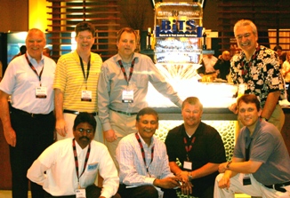
| BiTS
2009 Organizing Committee
|
Front:
Ila Pal (Antares Advanced Test Technologies), Rafiq Hussain
(AMD), Mark Murdza (Cascade Microtech),
Valts Treibergs (Everett Charles Technologies)
Back:
Paul Boyce (Advantage Specialist),
Owen Prillaman (TechConnect Sales), Steve Hamren
(Micron Systems Integration), Fred Taber (BiTS Workshop)
Not Pictured:
Morten Jensen (Intel), Mike Noel (Freescale),
Tim Swettlen (Intel), Joachim Moerbt (Advantest Europe), John Moore (Texas
Instruments), Kena Pegram (R&D
Circuits), Marc Knox (IBM) |
 |
|
|
|
Tutorial 1 |
SOCKETS
101: A BROAD AND DEEP SURVEY OF TEST INTERCONNECT SOLUTIONS |
2009tutorial1_diller.pdf
 (1.93 MB)
|
|
 |
|
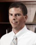
Jon Diller
Director of International Sales & Marketing
Interconnect Devices, Inc. |
Mr. Jon Diller is the Director of
International Sales & Marketing at Interconnect Devices, Inc. In his
15+ years of experience in applications engineering for Interconnect
Devices, Inc., Mr. Diller has worked around the globe on a variety of
test interconnect projects. He holds degrees from the University of Iowa
and Ottawa University.
|
|
This tutorial offered a comprehensive study of test
sockets. With an emphasis on socket technology, the role of the
socket in the test interface was defined from electrical and
mechanical perspectives. Plus, commercial aspects, some history and
a future roadmap were discussed. The many
options for electrical contacts, which are perhaps the most critical
factor in the success of a socket as a transparent interconnect,
were described and compared in detail. Their anatomies,
advantages, and vulnerabilities were made plain to attendees
regardless of their background and experience.
Likewise, various socket materials and their limitations
were
reviewed. The features which integrate the test socket with its
compression mechanism (be it manual lid or robotic test handler)
were covered to provide an understanding of how they shape the
socket platform.
This led naturally into how devices can be aligned within sockets,
which in turn carried the discussion into a comparison of various
techniques for alignment such as floating nests and strip test.
High-frequency behavior was touched upon
briefly, to the extent necessary for typical engineers to select
contacts and specify socket constructions. Finally, maintenance and life-tracking
was reviewed with an eye
toward better and more economical test strategies. Engineers who
attended this session, regardless of their experience with test
sockets, left with a fundamental and comprehensive
understanding of test sockets in terms of application,
specification, and selection. |
Who
should have attend
this tutorial:
Test engineers who are relatively new to the socket ‘world’
accelerated their knowledge of sockets, while veteran engineers gained new insights by having the opportunity to think outside of the
boundaries of their direct experience. Others, such as executives,
journalists, and academics, whose work takes them close to the
socket industry and seek a deeper understanding of the
socketing field and all its vagaries, found this tutorial just
what they need. |
|
|
Tutorial 2 |
"WHAT'S
THAT THING UNDER MY SOCKET?" |
2009tutorial2_bresnan.pdf
(1.74 MB)
|
|
 |
|
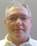
Tom Bresnan
Sales Manager R&D Circuits |
Mr. Tom Bresnan is the National Sales
Manager at R&D Circuits of South Plainfield, NJ. His more than 25 years of
Printed Circuit Board manufacturing experience includes positions in various
Engineering and Management roles for some of the world’s largest
manufacturers of complex Printed Circuit Boards, including Hadco, Multek and
Sanmina-SCI. He is a distinguished lifetime member of the IPC (a US based,
global trade organization representing the printed circuit industry)
Technical Activities Executive Committee, and has presented and published
numerous technical articles for the industry on MCM-L’s and advanced plating
capabilities. He resides in Colonia, NJ with his wife Joanne and sons, TJ
and Kyle.
|
| That
‘thing’ under your socket is a Printed Circuit Board (PCB) – a
critical part of your packaged test and/or burn-in solution. This
tutorial’s scope offered attendees an across the board examination of
those Printed Circuit Boards sitting under your socket. The focus
was
on learning about the attributes, materials and processes required
to produce the PCB’s used as test interface boards. In ‘bringing the
Printed Circuit Board shop to the tutorial hall’, a better
understanding of the challenges you and your PCB vendors face was
attained.
A brief history of the PCB or PWB (Printed
Circuit/Wiring Board) industry was covered, specifically in relation
to the ATE industry. Next detailed discussions on pitch, layer
count, board thickness and via drill hole diameter (to name but a
few of the critical attributes of today’s interface boards) on
manufacturability and cost was explored. Additionally, the many
options currently available for materials, and how those options may
be shrinking (as is device pitch!) were examined.
That was followed by a detailed explanation of the PWB manufacturing process - from raw materials through finished
product, including new visual aids and a hands-on exhibit of a PWB
in all its process stages.
Last, but certainly not least, the quality and
performance characteristics you can demand of your supplier(s) was
analyzed. Even with today’s boards becoming more crowded (with
components) and pitch and pin counts driving attributes ever
smaller, there are ways to verify and validate the quality of your
interface boards with your suppliers. Attendees learned how, with samples
of data gathered over years of process development, characterization
and verification.
|
Who should have attend this
tutorial:
Test Engineers & technicians (and others) who wanted more detailed
knowledge of just what a printed circuit board is (and isn’t) will
find this an excellent tutorial on Printed Circuit Board design and
manufacturing. This is a rare opportunity where attendees, whose
work in the test and burn-in arena benefits from a deeper
understanding of Printed Circuit Board technology, participated
in a concentrated tutorial covering such a key topic area, and came
away with a new-found understanding of PCB technology capabilities
and limitations. |
|
|
|
Invited
Speaker |
BiTS
and Pieces– Past, Present and Future |
2009forster.pdf
(2.09 MB)
|
|
 |
|
Dr. James Forster
Chief Technical Officer
Antares Advanced Test Technologies |
|
|
|
The BiTS Workshop is the world’s premier event dedicated to
providing a forum for the latest information about test and burn-in socketing
and related fields. It has become the annual event for those involved in the
“backend” of semiconductor processing and draws attendees and exhibitors from
around the world for learning and networking. The workshop has been held in the
Phoenix area since its inception in 2000.
This year represents a significant milestone as the workshop
celebrates its 10th meeting. During the history of BiTS we have experienced good
food, good company and excellent and perceptive presentations. While all the
presentations are available on the BiTS website, perhaps the 10th anniversary is
a good time to take a little time to reflect on some of the previous
presentations.
The BiTS Workshop’s archives are a tremendous source of
information. This presentation will re-examine some of the presentations from
the previous 9 workshops. Specific papers will be highlighted and some “sense”
and “perspective” given – the past presentations will be dusted-off and a light
shone into this library of information.
After looking backward, a look forward will examine packaging
trends and the potential issues the audience will have to face in the coming
years.
Dr. Forster is the Chief Technical Officer for Antares
Advanced Test Technologies. He joined the Wells-CTI Divison of Antares in 2005
as a Materials Technology Manager. Previously he held a variety of management
positions with the Sensors and Controls Group of Texas Instruments. He has
authored more than 25 technical publications including several on the challenges
of burn-in sockets. A holder of 18 U.S. patents, Dr. Forster earned his B.Sc
with honors in Mechanical Engineering in England at the University of Manchester
Institute of Science and Technology and his Masters and Doctorate in Mechanical
Engineering at McMaster University in Hamilton, Ontario, Canada.
|
|
Invited
Speaker |
Opportunity or Disaster - What You Need to do for the Next 10 Years |
2009pfaff.pdf
(86 KB)
|
|
 |
|
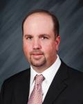
David Pfaff
President
Plastronics Socket Company |
|
As BiTS celebrates its 10th anniversary, the industry is being
challenged with unprecedented global and business issues. Companies need to
take action, but what should they do? Sometimes the
wrong action is worse than no action at all. This talk will discuss how not
to get caught up in the current pandemonium but to stay focused on what is
important for your business. You’ll be taught powerful ideas you can
implement today to ensure your company successfully makes it to BiTS 2018.
Mr. Pfaff is President of Plastronics Socket Company. He has
run Plastronics Socket Company, a fully integrated design, molder and
manufacturer of burn-in sockets, for over 10 years. Mr. Pfaff graduated from
Pomona College and has a MBA from the University of Texas at Austin. He lives in
Irving, Texas, with his wife and two beautiful children. |
|
|
BiTS
2009 TECHNICAL PROGRAM - SESSIONS |
|
Opening
Remarks |
|
2009welcome.pdf
(455 KB)
|
| Welcoming remarks from the General
Chair |
|
|
BiTS 2009 Keynote
Address
|
IC
Packaging: Global Trends, Technologies and Next Generation
3D Solutions |
2009prior.pdf
(734 KB)
|
|
 |
|
Brandon Prior
Senior Consultant
Prismark Partners |
|
IC packaging solutions have been evolving in many
ways that were forecast, and in some ways not predicted by any
analysts. This presentation looks at the recent trends of IC
packages in terms of package type, pitch, and integration for
multi-chip and 3D solutions. In preparing for the next decade of
innovations, this brief synopsis provides a forecast for current
advanced packages, and a look into future developments in 3D and
package integration that may have an impact on overall test
strategies and challenges going forward.
Mr. Brandon Prior joined Prismark Partners in 1996
and is the editor of Prismark’s Semiconductor and Packaging
Quarterly Report. He works with the leading component, equipment and
material providers to provide custom market and technology research
in the area of IC packaging. Mr. Prior earned BA and BE degrees from
Dartmouth College and the Thayer School of Engineering in Hanover
NH. |
|
|
|
Session 1 |
Living
the High Life (High Current & Power) |
2009s1.pdf
(1.65 MB)
|
|
This session offers a representative look at the "high life" of those
dealing with high power and high current issues in the BiTS environment. The
kickoff paper features analysis and insight related to current carrying
capabilities of small metal conductors in response to current pulses. Then
it’s an examination of the role and impact of decoupling capacitor placement
as it relates to efficient power delivery. The session then follows the
power delivery path into the realm of socket contacts with a look into the
socket contact and the associated contact to product interface as they are
both pushed to operate at very high current densities. The closing
“highlight” is an overview of the issues associated with socketing high
power devices, spanning from power delivery issues to related thermal
issues. |
"Pulsed
Current-Carrying Capacity of Small Metallic Conductors as Applied to
Device Test"
 |
Harlan Faller
Johnstech International Corporation |
|
|
| "Power Integrity
Ingenuity at Test" |
Abram Detofsky
Intel Corporation |
Omer Vikinski
Intel Corporation |
Shaul Lupo
Intel Corporation |
Tim Swettlen
Intel Corporation |
|
|
| "Moore or Less:
Effects of Higher Currents on Socket Life" |
Kevin DeFord
Interconnect devices, Inc. |
|
|
| "Design
Considerations in Socketing High Power Devices" |
Jec
Sangalang
Yamaichi Electronics USA Inc. |
Mike Noel
Freescale |
|
|
BiTS 2009 Distinguished Speaker |
Breaking Traditional Boundaries - OUR Industry Challenges at Test |
2009shahriari.pdf
(575 KB)
|
|
 |
|
Navid Shahriari
Director of STTD
Intel Corporation |
|
Success in the semiconductor market is never predictable
but it always involves being faster, cheaper or better than your
competition. This maxim holds especially true when it comes to
microprocessor test. While Moore’s Law has spawned a profusion of
product features and functions through ever cheaper and abundant
transistors, it has left test with increasing complexity and cost.
Additionally, market forces necessitate ever-smaller form factors as
mobile products become ubiquitous. This combination of shrinking
geometry, increasing bandwidth and expanding features creates a
confluence of mechanical, electrical and thermal challenges that run
head-on into a severely cost constrained environment in the midst of an
economic downturn.
Meeting these stringent technical challenges while providing cost
effective solutions, requires a collaborative response from the whole
industry. Customers and suppliers alike. An outlook on the key
technology drivers, leadtime, and total test costs, as well as what can
be done between the suppliers and customers, to accelerate improvements
beyond normal evolution, will be shared with the audience.
Mr. Shahriari is the Director of STTD (Sort Test
Technology Development) at Intel Corporation. Since 1989, he has held
several engineering and engineering management positions in test
equipment, process development, product engineering, and supplier
development at Intel. He’s a founding member of the STTD group, which
originated in 1993. He earned his Bachelor of Science and Masters Degree
from Arizona State University.
|
|
Poster Session 1 |
|
2009p1.pdf
(978 KB)
|
|
This is the first of two poster sessions.
Poster Sessions offered an additional means for scientific
communications between authors and attendees. With their interactive nature,
Poster Sessions provided authors and attendees with the opportunity to share
and explore ideas more deeply, yet less formally, than a podium
presentation. |
"Contact Challenges
with Leadless Devices"
 |
Justin Toops
Interconnect Devices, Inc. |
Kiley Beard
Interconnect Devices, Inc. |
John Diller
Interconnect Devices, Inc. |
| "Interconnect
Technology: Is There Really Such a Thing as a Sweet Spot?" |
Paul Schubring
Plastronics |
Praba Prabakaran
Antares Advanced Test Technologies |
|
| "A Fast
Optimization Approach which Integrates Mechanical & Electrical
Performance into High Speed Socket Design" |
Dr. Yen-Chih Chang
Hon Hai Precision Ind. Co. Ltd. |
Andrew Gattuso
Foxconn Electronics, Inc. |
|
| "High Performance
Electrical Contact For 0.3-0.4 mm Contact Pitch" |
SM Low
ADE Technologies |
Che-Yu Li
Che-Yu Li & Co. |
Adam Hopper
Protos Electronics |
Tia Korhonen
Che-Yu Li & Co. |
|
|
|
|
Session
2 |
Novel Approaches to Socket
Design |
2009s2.pdf
(1.43 MB)
|
|
Among the significant socketing challenges we are faced with today are
tighter alignment requirements for fine pitch devices, the emerging field of
package on package contacting, not to mention high power requirements and
the ever-present relentless pressure to reduce lead time. In this session we
learn more about some of the newest developments
in socket technology that are targeted at addressing these issues. |
| "PoP Contactor -
Challenges and Solutions" |
Jiachun
(Frank) Zhou
Antares Advanced Test Tech. |
Siang Soh
Antares Advanced Test Tech. |
David B.
Bogardus
Antares Advanced Test Tech. |
Brian L.
Hahn
Antares Advanced Test Tech. |
|
|
| "A Bias Clip
System for the IC Alignment" |
Hide Furukawa
Sensata Technologies, Inc. |
Hideyuki Takahashi
Sensata Technologies Japan |
|
| "High
Temperature, Fast Turnaround Modular Burn-in Socket " |
Rick A. Taylor
EP Ants GmbH |
Stefan Lang
EP Ants GmbH |
Ernie Frain
EP Ants GmbH |
| "New PTB / High
Power Kelvin Test Socket Concept" |
Gerhard
Gschwendtberger
Multitest Elektronische Systeme GmbH |
|
|
|
|
Session 3 |
Adventures
in Test & Burn-in Operations |
2009s3.pdf
(1.48 MB)
|
| As
packaged devices continue to grow in complexity, test and burn-in challenges
increase as well. With that, operational costs and the efficiency of
semiconductor operations become critical factors in maintaining
profitability. Higher power, higher pin count, package size and packaged
device complexity drive the need to increase operational efficiency and
develop better techniques to ensure success in a semiconductor manufacturing
environment. This session's authors share their novel ideas on how to
improve your operations in the areas of PCB tuning, electrical bias
techniques, contactor tracking, and parallel test solutions. |
| "Parallel Logic
Test Interface Solutions" |
YH Jeon
TSE |
Sang-Il Kwon
TSE |
Gary Westendorf
Pragmatics |
Chris Mack
Pragmatics |
|
|
| "CID: A New
Breakthrough Solution for Contactor Hardware Tracking" |
Jonathan Mondero
Texas Instruments Philippines |
Kevin Tiernan
Texas Instruments Houston |
Mike Guenther
Texas Instruments Houston |
Eugene
Batilo
Everett Charles Technologies – STG Singapore |
|
| "Mechanical
Reliability Test as Part of Final Test of a Packaged Chip" |
Tia Korhonen
Che-Yu Li & Co. |
Che-Yu Li
Che-Yu Li & Co. |
Tim Wooden
Protos Electronics |
SM Low
ADE Technologies |
|
|
| "Substrate Bias:
Application in Final Test and Burn-in of High-Power CPU's" |
Max Paransky
Texas Instruments |
|
|
|
|
Poster Session 2 |
|
2009p2.pdf
(989 KB)
|
|
This is the second of two poster sessions.
Poster Sessions offered an additional means for scientific
communications between authors and attendees. With their interactive nature,
Poster Sessions provided authors and attendees with the opportunity to share
and explore ideas more deeply, yet less formally, than a podium
presentation. |
| “Elastomer Contact
System for ATE - Innovation to the "Core" ” |
Tony Smith
Phoenix Test Arrays |
Frank Bumb
Phoenix Test Arrays |
Jack Pereschuk
Phoenix Test Arrays |
Ila Pal
Antares Advanced Test Tech. |
Roni Awale
Antares Advanced Test Tech. |
|
| “The Development of a
PB Free Test Socket” |
Hidekazu "Hide" Miura
MJC Electronics Corp. |
Fred Megna
MJC Electronics Corp. |
|
| “Kelvin Testing of
BGA Devices - Packaged and Wafer-Scale” |
Jim Brandes
Everett Charles Technologies |
Valts
Treibergs
Everett Charles Technologies |
|
|
|
Session 4 |
PCBs – More Than Just Boards |
2009s4.pdf
(2.38 MB)
|
|
Within final test and burn-in of packaged devices, PCBs play a major role on
yield, test results and cost. Therefore the performance of the electrical
path as well as the mechanical capabilities of PCBs must be taken into
account. In this session PCBs are viewed from different angles to comply
with the needs of future testing: design, manufacturing and operation. The
authors reflect on simulation of PCBs and contactor parasitics within the
system up to the pin of the device, as well as on the necessity of cost
reduction by selecting cost efficient BIB interconnection methods. In
addition the manufacturability of fine geometric structures is outlined. |
"Tuning a
PCB/Contactor System to Your Device"
 |
Ryan Satrom
Everett Charles Technologies |
|
|
"A
Novel Redesign of BI System Interconnects Results in Major BIB Cost
Reduction for Day-to-Day Operations"
 |
Bob Jemison
RJI Technical Sales |
|
|
| "Advances
in Plating Technology, Reliable High Aspect Ratio Holes" |
Thomas N.
Bresnan
R&D Circuits |
|
|
|
|
Session 5 |
A Salmagundi of Socket Science |
2009s5.pdf
(2.51 MB)
|
| A
salmagundi? Not sure what a salmagundi is? Hint: this session has mix of 4
diverse topics. They offer an insight into the broad range of subjects that
encompass the socketing field. You’ll hear about an
innovative technique to manage fine pitch testing, using modeling to
optimize performance, the motivation and methods to conduct burn-in at the
wafer level and conducting comparative socket evaluation experiments. |
| "Performance
Studies on Space Transformer Structures" |
Roger Weiss
Paricon Technologies Corp. |
|
|
| "Design
& Test of Very High Bandwidth QFN/QFP Sockets" |
James Zhou
Antares Advanced Test Tech. |
Ila Pal
Antares Advanced Test Tech. |
Dr. James
Forster
Antares Advanced Test Tech. |
Jiachun
(Frank) Zhou
Antares Advanced Test Tech. |
Steve Davis
Antares Advanced Test Tech. |
Dima
Alzoubaidi
Antares Advanced Test Tech. |
| "Improving
Your Test System Performance in High Frequency Applications" |
Jeff Sherry
Johnstech International |
Michael Voo
Avago Technologies |
|
|
"Wafer-Level Burn-In of Hall-Effect Sensors" |
Steve Steps
Aehr Test Systems |
Jochen
Seidler
Micronas GmbH |
|
|
|
|
Session 6 |
Studies
and Evaluations of Electrical Contacts |
2009s6.pdf
(7.86 MB)
|
|
Making good electrical contact is a core focus of test socket solutions
today, and organizations across the industry invest endless amounts of
resources into studying and evaluating electrical contacts in efforts to
optimize performance, reliability, and cost. This session presents four
angles into electrical contact challenges in an ever-challenging test
environment. |
| "Test on
Ball" |
Khaled
Elmadbouly
Antares Advanced Test Tech. |
Ila Pal
Antares Advanced Test Tech. |
Cody Jacob
Antares Advanced Test Tech. |
Dr. James Forster
Antares Advanced Test Tech. |
|
|
| "Contacting
Pb-free Finishes - A Study of the Effects of Different Lead Finishes
on the CRES and Reliability of a QFP Contact" |
Dr. James
Forster
Antares Advanced Test Tech. |
Kazumasa Sato
Antares Advanced Test Tech. |
Don Hewer
ST-Microelectronics (Malta) |
"Current-Voltage
Nonlinearities in Test Socket Contacts"
 |
Gert
Hohenwarter
GateWave Northern, Inc. |
|
|
| "Evaluation
of Different Price-Point Spring Pin Contactors for an RF
Application" |
James
Migliaccio
RF Micro Devices |
John Capwell
RF Micro Devices |
|
|
|
Session 7 |
Advancements
& Innovations in Socket Materials |
2009s7.pdf
(310 KB)
|
|
Advancements in packaged electronics, like larger size, very high I/O counts
and tighter pitches have placed increased stress on selecting the right
materials for socket bodies and electrical contacts. Socketing these
packages demand plastics that can handle thinner side-walls, have higher
moldability, and maintain better dimensional stability, plus requiring the
metals for electrical contacts to have higher strength, formability and
electrical conductivity. In this session, learn about
choosing socket materials but also become acquainted with their recent
advancements and innovations. |
"New
Performance-Enhanced Cu-Be Strip Products for Burn-in Test Socket
Applications"
 |
John C. Harkness
Brush Wellman Inc. |
|
|
| "The Evolution &
Evaluation of Plastics Materials in Burn-in & Test Applications " |
Dana Scott
Quadrant EPP |
Scott Williams
Quadrant EPP |
|
|
|
Awards
/ Closing Remarks
|
2009closing.pdf
(291 KB) |
|
|
|
|
|
Page last modified
12/23/09
|
 |
BiTS WorkshopTM is a production of
BiTS Workshop LLC |
|