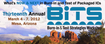
BiTS
is the world's premier workshop dedicated to
providing a forum for the latest information
about burn-in and test socketing, and related
fields.
At BiTS you'll find a comprehensive technical
program, exhibits of the latest products and
services, and many opportunities to meet,
network and explore ideas with other test and
burn-in socketing professionals.
Click here if you need the latest Acrobat(R) reader
from Adobe(R):
or
for an alternate free PDF
viewer, download the latest
Sumatra PDF
It is FAST!
BiTS
2012
ARCHIVE PAGES
COPYRIGHT NOTICE
The papers in this publication
comprise the proceedings of the 2012 BiTS Workshop. They reflect the authors’
opinions and are reproduced here as presented
with occasional minor edits. Their inclusion in
this publication does not constitute an endorsement by the BiTS Workshop, the
sponsors, BiTS Workshop LLC, or the authors.
There is NO copyright protection claimed by this publication; some tutorials may
be copyrighted.
However, each presentation is the work of the authors and their respective
companies: as such, it is strongly suggested that any use reflect proper
acknowledgement to the appropriate source. Any questions regarding the use of
any materials presented should be directed to the author/s or their companies.
All photographs on this page are copyrighted by BiTS Workshop LLC. The BiTS logo
and ‘Burn-in & Test Strategies Workshop’ are trademarks of BiTS Workshop LLC.
Technical Program
Once again,
the BiTS Workshop offered a robust and riveting program featuring 30+
papers presented during 7 podium and two poster sessions covering a host
of test and burn-in related topics from a worldwide representation of
authors
A TechTalk session
started the workshop off building
on his 2006 “Geometric Dimensioning and Tolerancing” primer tutorial, which
regularly tops the BiTS charts as most
frequently downloaded archived
presentation, Thomas Allsup returned to
further enlighten BiTS Workshop
attendees with an exciting look at GD&T
fundamentals, an explanation of changes
in the new ASME Y14.5-2009 standard, and
an in-depth examination of actual
semiconductor GD&T drawing examples.
Dr. Roland Timsit returned for
a refresher Tutorial on the “Fundamental Properties of
Electrical Contacts”. The seminar addressed how contact force and the
mechanical properties of contact materials affect both contact
resistance and the electrical/mechanical integrity of an electrical
contact device.
Distinguished Speakers,
John Morrissey and Mark Hopman from Intel share key tooling business
trends, challenges and what can be done to enable future opportunity and growth
in the test tooling industry.
Keynote Speaker, Jim
Feldhan of Semico Research presented the Semico roadmap to 3D
packaging, the end products that adopt 3D and how that adoption will evolve over
time.
Fred Taber shared some socket market data with BiTS participants mined from recent Fleck Research
research reports.
BiTS EXPO
2012
47 exhibitors, from socketing and related industries, exhibited their products and services
during breaks in the technical program. Click
HERE for the exhibitor list of BiTS EXPO 2012.
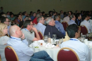
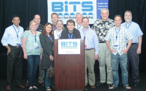
Participants
BiTS 2012 brought together well over 300 participants,
including nearly 250 full conference attendees, and 47 exhibitors from
around the world, representing end users and suppliers of sockets, boards,
burn-in systems, handlers, packages and other related equipment, materials and
services.
Front:
Kena Pegram (Phoenix Test Arrays), CY Lai
(Test Tooling Solutions) , John Hartstein (Wells-CTI),
Valts Treibergs (Multitest),
Mike Noel (Freescale), Tim Swettlen (Intel)
Back:
Rafiq Hussain (AMD),
Marc Knox (IBM),Morton
Jensen (Intel),
Paul Boyce (Advantage Specialist), Fred Taber (BiTS Workshop),
John Moore (Texas Instruments)
,
Not pictured:
Joachin Moerbt (Advantest Europe) ,
Owen Prillaman (Tech-Connect Sales, Ila Pal (Ironwood Electronics)
TUTORIAL
DAY
Sunday, March 4, 2012
TechTalk
Geometric Dimensioning and Tolerancing for Burn-In and Test Professionals
Geometric Dimensioning and Tolerances (GD&T) is the
common language used to describe the allowable variances of manufactured feature
sizes, shapes, and locations beyond that which can be controlled by regular
rectilinear and angular dimensions and tolerances.
Semiconductor component and socket manufacturer drawings both
use GD&T to insure their respective components fit and function mechanically
together.
The “How to Spell GD&T” tutorial previously presented at BiTS
provided a detailed primer of how to read GD&T symbols on drawings and provides
an introduction to this tutorial.
This new tutorial is presented in three sections: Section one
provides a highly abbreviated “How to Spell GD&T” review of the fundamentals of
GD&T, Section two explains the first changes to the ASME Y14.5 standard in
fifteen years, particularly where those changes impact semiconductor
professionals, and Section three contains a series of public domain
semiconductor component drawings that will be carefully dissected to explain how
GD&T was used correctly and incorrectly.
Thomas Allsup is the Managing
Partner of Anida Technologies, a Dallas based design contract services
company and has twenty four years of experience in various engineering
roles. Thomas earned a BSME from Oklahoma State University and an MSME
from the University of Texas at Arlington. He has experience in the
design of fixtures for back-end semiconductor processes, including the
design and manufacture of custom semiconductor burn-in and test sockets,
and provides training in many technical subjects including CAD, GD&T,
and DFMA.
Dr. Roland S. Timsit
President Timron Advanced Connector Technologies
An
interface between two solids is generated by contact between
protruding surface asperities on each of the contacting bodies, so
that mechanical contact is actually established at a discrete number
of contact spots. Because these spots are tiny, the area of true
contact is very small and electrical current passing through the
interface is highly constricted at these spots. Constriction of the
current gives rise to contact resistance.
The seminar addresses how contact force and the
mechanical properties of contact materials affect both contact
resistance and the electrical/mechanical integrity of an electrical
contact device. Selected contact properties of materials and
electroplates such as gold, tin and silver are reviewed. The
deleterious effects of contaminant and corrosion surface films, and
other mechanisms such as mechanical wear and fretting corrosion,
that conspire to eliminate electrical contact spots, are described.
The nefarious effects of these mechanisms can often act rapidly,
with ensuing catastrophic failure, in devices where the contact
force is small such as in MEMS. The effect of signal frequency on
contact resistance will also be addressed.
Dr. Timsit spent 20 years in R&D in
the aluminum industry where he focused on power connector design,
aluminum surface modification, connector cable alloys, lubrication,
brazing and metalworking.
In 1994, he joined AMP Inc. (now TE
Connectivity/Tyco Electronics) and led technology development for the
AMP Power Technology Division as Chief Technologist.
Dr. Timsit is a recipient of the IEEE Ragnar Holm
Scientific Award for innovative research in electrical contacts. He is
also a recipient of four international awards relating to electrical
contacts and metal joining. He has authored of over 130 papers, including
Chapter I of the IEEE Book Publication "Electric Contacts: Theory and
Applications", and holds 15 patents.
Over the last thirteen years, Dr. Timsit has served as
President of Timron Scientific Consulting Inc., Toronto, Canada, a
provider of technology support to electronic/electrical connector
manufacturers and users in the Americas, Europe and Asia..
This year’s Marketplace segment of the BiTS program, offered 2 new and
unique topics and reprises 2011's report on the business side of
sockets with fresh data.
"Where It’s At -
Understanding the Geography of the BiTS Market"
Mr. Feldhan provided a brief economic overview
along with Semico’s Semiconductor Forecast. As ICs become more complicated and
push the technology roadmap, system performance and chip to chip interaction is
becoming a limiting factor. The result, test and packaging is coming to the
forefront. 2.5D and 3D package offer great advantages, yet there are still
technical issue to overcome. Mr. Feldhan presented the Semico roadmap to 3D
packaging, the end products that adopt 3D and how that adoption will evolve over
time.
Jim Feldhan founded Semico Research
in 1994. A 20-year veteran of the semiconductor industry, he brings his
management, forecasting and modeling expertise to Semico, along with a
reputation for quality research. Jim designed and developed the research
methodologies and report structures, which are the basis for Semico’s
Custom Research and Portfolio Services. He also develops Semico’s
overall economic outlook as well as performing various semiconductor
consulting and forecasting. With a focus on quality, Semico Research has
grown to be the largest semiconductor-focused consulting and research
firm.
Jim was formerly the Executive Vice-President and
General Manager at In-Stat. As a member of the start-up team there, he
was responsible for the design, methodologies, and implementation of
research that was the basis for the Semiconductor Services.
Mr. Feldhan also held various management, marketing
and manufacturing positions at GTE Microcircuits and Greyhound/Dial
Corporation. He received a BS in Business with a minor in Chemistry from
the University of Arizona and a MS in Marketing focusing on quantitative
statistics and market research from the University of Arizona.
What do today's burn-in process, power delivery efficiency, DUT temperature
control, pin characterization and socket qualification all have in common?
They're all being challenged by smaller geometries, increased power with
localized densities and thermal conditions, all compounded with a need to
produce solutions in less time at lower cost. Speakers in this session have
come up with some innovative solutions such as a novel approach to
addressing burn-in challenges with a thermal interface material, managing
electrical, mechanical and thermal challenges for high current
implementation in a temperature-humidity system, managing DUT temperature
using LN2 injection and the development of a programmable tool to
characterize socket pins.
"Burn-in Process
Thermal Challenges With High End Applications"
Oswaldo Chacon
IBM Canada Ltd.
Alexandre Leblanc
IBM Canada Ltd.
Martin Laliberté
IBM Canada Ltd.
Benoît Foisy
IBM Canada Ltd.
"High Current
Implementation in a Temperature-Humidity System"
John Pioroda
Incal Technology
Naveed Syed
Incal Technology
"DUT Temperature
Control Using LN2 Injection"
Chad Turner
Texas Instruments
Joseph Mayfield
Texas Instruments
Nolan Riley
Texas Instruments
"Sophisticated
Tool for Pin Characterization & Socket Qualification"
Praveen
Kumar Ramamoorthy
Intel Corporation
K. W. Low
Intel Corporation
BiTS 2012 Distinguished Speakers
Package
Level Test Challenges – Delivering More Than a Technology
John Morrissey ATCED Test
Tooling Manager Intel Corporation
Mark Hopman STTD Wafer Test &
Tooling Manager Intel Corporation
Moore’s law continues to set the pace for the Microprocessor
industry driving transistor density, performance and rich capabilities even as
ASPs drift down. Test capital has stretched to keep up through improved
parallelism, advanced architectures and in-field configurability while test
tooling quality, lead time and cost are starting to fall behind. New technology
needs will continue to challenge test tooling but are more evolutionary in
nature while the business drivers have grown to be critical.
We are seeing an inflection in the test tooling industry’s
future where traditional test strategies will evolve. Quality, lead time and
cost will dominate tooling choices and be the future engine to enable
quicker time to market, a more nimble business and improved cost
competitiveness. Test tooling has moved from a commodity to an integral
business enabler. Tight collaboration between supplier and customer will be
paramount. We share key tooling business trends, challenges and what
can be done to enable future opportunity and growth in this industry.
Mr. Morrissey manages the test tooling team within Intel’s Assembly Test
Capital Equipment Development (ATCED) organization. In his 18 years at
Intel, he has spent the majority of his time managing supplier teams and
ensuring Intel’s factory needs are met on time and within expectations.
Mr. Hopman leads Intel’s Sort
Module and Package Test Tooling technology development team. His 25 year
career at Intel has focused on Product Engineering, Sort Factory
Management, and test module and tooling development.
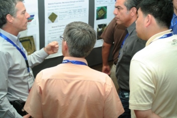
Sure, podium presentations are great, but sometimes it’s
nice to have a one-on-one chat with the author. And, we all wonder: how many
people are inclined to ask those provocative questions in front of the whole
audience?
With a variety of topics being addressed, poster sessions
offer the perfect opportunity for authors and attendees to interact directly
and even share ideas in an informal setting while enjoying some
refreshments.
"IM Material for
High Pin Count Socket"
Jiachun
(Frank) Zhou
Interconnect Devices, Inc.
Dexian
Liu
Interconnect Devices, Inc.
Khaled
Elmadbouly
Interconnect Devices, Inc.
Brad Henry
Interconnect Devices, Inc.
Kevin DeFord
Interconnect Devices, Inc.
"Socket Spring
Probes - Degradation Experiments"
Shaul Lupo
Intel Israel
“Low Force SuperButton® Connector Technology”
Amit Varma
High Connection Density, Inc.
“Use of Conical Inductors for Load Boards Testing”
It's amazing what streamlining burn-in and test operations and processes can
do for your bottom line. This session focuses on optimized methods developed
to improve throughput, increase yields and extend the life of the equipment
itself. First, you'll hear about using test-in-tray methods to effectively
test devices under rigorous thermal regimes and power levels. The second
speaker will explain an alternative manufacturing method for rapid
prototyping of test socket. A presentation on optimized online socket
cleaning promises improved yields and reduced retest. Wrapping up the
session will be a paper on how alternative coatings can improve contact
life.
"High Performance
Testing in Test-in-Tray Format"
Thomas H. Di
Stefano
Centipede Systems
"Using
Alternate Manufacturing Methods for Rapid Prototyping of Test
Sockets"
James Migliaccio
RF Micro Devices
"Consistent
Online Test Socket Cleaning for First Pass Yield Stability and
Reduced Retest"
Jerry Broz, Ph.D.
International Test Solutions, Inc.
Bret Humphrey
International Test Solutions, Inc.
"Achieving
Extreme Contact Life Through the Application of Alternative
Coatings"
What good is it to have optimized test devices if the characterization and
analysis processes aren't up to speed as well? This session focuses on the
whole picture. We open with methods for taking device specifications and
translating them into test contactor requirements to reduce the impact of
testing the device in the contactor. Next we'll move on to the challenges of
balancing signal integrity with power integrity through the socket and PC
board. The session wraps up with two presentations investigating parameters;
the first discusses key parameters of pulse current testing and their
significance and the second shares some crucial parameters in thermal
simulations.
"Understanding
Specs to Better Simulate Solder to Board Performance"
Jeff Sherry
Johnstech International
"Mitigating Test
Interconnect Issues for the Next Generation of High Speed, High
Power Devices"
Thomas P. Warwick
R&D Circuits, Inc.
Al Seier
R&D Circuits, Inc.
"Pulse Current
Testing: Parameters and Their Significance"
Sure, podium presentations are great, but sometimes it’s nice to have a
one-on-one chat with the author. And, we all wonder: how many people are
inclined to ask those provocative questions in front of the whole audience?
With a variety of topics being addressed, poster sessions offer the perfect
opportunity for authors and attendees to interact directly and even share
ideas in an informal setting while enjoying some refreshments.
"Novel
Approach to Detect and Diagnose Load Board Problems Early in the
Production Flow"
Maroon
Maroon
Intel Corporation
Gustavo
Cozacov
Intel Corporation
"Development of Pressure Sensitive Conductive Rubber (eM-PCR® /HAH-PCR®)"
Josh Jin
WinWay Technology Co., Ltd.
Hiroe Mochizuki
WinWay Technology Co., Ltd.
Jack Liang
WinWay Technology Co., Ltd.
Daisuke Yamada
JMT Microtech Inc.
Kazuhiro Chishima
JMT Microtech Inc.
Noriyuki Takeda
JMT Microtech Inc.
"BGA
Spring Probe for Fine Pitch and High Current"
For many socket and probe card manufacturers the pins are the secret sauce,
especially when performing burn-in and test on today's devices that have
increasingly finer pitch and smaller geometries. This session will feature
three presentations offering different contact solutions. The first speaker
presents a new technique for fine pitch applications that integrates a short
wiping stroke. Next up is a high-volume low-cost stamped spring probe in
development for burn-in sockets. The session closes with a presentation on a
simple, yet effective contact pin geometry.
It just wouldn't be a BiTS Workshop without a session devoted entirely to
novel socket designs. Every year, there are new devices on the market and
ever critical factors like witness marks on smaller solder balls and minimum
contact force that need a socket designed specifically for them. The three
papers in this session address three distinctly different socket
applications. The first talks to spring probes for fine pitch, then the
second paper reviews the heat path for a device mounted in a socket and
discusses the important variables in a thermal analysis. Lastly, we'll
examine a unique design for of a coaxial socket.
"Are Spring
Contact Probes Valid at Fine Pitch?"
Dr. Jiachun (Frank) Zhou
Interconnect Devices, Inc.
Jon Diller
Interconnect Devices, Inc.
"Evaluation
and Optimization of the Thermal Performance of a Socketed Device for
an HTOL Application - Considerations in the selection of a socket
for a plastic molded, thermal enhanced package"
Power delivery and signal integrity have become increasingly important
issues in device testing, especially for today's mobile electronics that
require more of both to achieve the levels of functionality expected by
consumers. As a result, they are becoming some of the greatest challenges in
designing test interfaces. In this session, presenters report on a number of
specific developments that address these challenges. The first presentation
will address the point of diminishing returns on socket pin length from a
signal integrity perspective. Next, we'll learn about the anatomy of PCB
vias in single-ended and differential signal paths. The third speaker will
offer solutions for improving power delivery in the test interface. Finally,
innovative interconnect evaluation metrics for design optimization will be
explained.
"Point
of Diminishing Returns on Socket Pin Length From a Signal Integrity
Perspective"
Sasha N.
Oster
Intel Corporation
Sermet Akbay
Intel Corporation
"The Anatomy of PCB Vias in Single-ended and Differential
Signal Paths"
Zaven Tashjian
Circuit Spectrum, Inc.
Kevin Chan
Circuit Spectrum, Inc.
"Improving Power Delivery in the Test Interface"
Ryan Satrom
Multitest
"New Interconnect Evaluation Metrics for Design Optimization"
When you think about it, advanced materials are the steroids of the device
testing world. The right material can often make the impossible possible. In
this session, we hear about the improvements three innovative materials make
to previous technologies. The first presenter introduces a new socket
material that improves high frequency performance, then the second speaker
examines socket contact plating and the impact on contact resistance in a
burn-in environment. The final presenter talks about developing clad alloys
for manufacturing test and burn-in sockets that better withstand the stress
relaxation induced by high temperatures without sacrificing strength and
performance.
"Fully Impedance
Controlled Socket With IM Material"
Jiachun
(Frank) Zhou
IDI, Smiths Group
Dexian
Liu
IDI, Smiths Group
Khaled
Elmadbouly
IDI, Smiths Group
Brad Henry
IDI, Smiths Group
Kevin DeFord
IDI, Smiths Group
"Socket Contact Plating and the Impact on Contact Resistance in
a Burn-in Environment"
Mike Noel
Freescale Semiconductor
Shawn Toth
Enplas Semiconductor Peripheral Corp.
"Using Clad Alloys to Make High Temperature Burn-in and Test
Sockets"
Terry Morinari
Enplas Semiconductor Peripheral Corp.