' . "\n"; echo ' ' . "\n"; echo "
\n"; } ?>
TestConX China 2018 Advance Program

Join us for the fourth annual BiTS event in China focused on solutions for electronic test!
Everything from wafer to final and beyond including module, system-level, and product test.

TestConX China will feature technical presentations highlighting new regional presentations along with presentations from BiTS award winning authors.

Connecting electronic test professionals to solutions

Over the course of its twenty-year history, BiTS has established itself as the preeminent event for test consumables, test cell integration, and test operations. BiTS has also grown from packaged semiconductor “final” test and burn-in to encompass all practical aspects of electronics testing including validation, advanced packaging testing, system level test, module test, and finished product test. Participation has grown from the semiconductor industry to the electronic manufacturing services (EMS) industry. The new TestConX name reflects this broader scope and increased reach.

Each one-day event will deliver our core values of LEARN, EXPLORE, and SHARE. There will be plenty to LEARN in a strong technical program that includes a keynote, a market overview, and nine excellent technical presentations. The learning will continue as you EXPLORE the TestConX EXPO where local and international vendors exhibit the latest in test hardware, equipment, and consumables. Lastly, TestConX has been structured to encourage networking with over three hundred of your colleagues – from the scheduled breaks to the buffet lunch – to enable you to SHARE your challenges and solutions with your industry peers. The person you meet at lunch may have the exact solution you are looking for!

New for 2018: This year there will be two TestConX China events: Tuesday October 23 at the Hilton Hotel in Suzhou and Thursday October 25 at the Raytour Venice Hotel in Shenzhen.

Please see the detailed agenda below for this great event!

TestConX China will be held at:

Tuesday October 23
Hilton Suzhou - Suzhou, China
275 SUZHOU AVE EAST INDUSTRIAL PARK
SUZHOU, 215028, CHINA
+86-512-62928888

Suzhou TestConX EXPO Directory


Thursday October 25
Raytour Venice Hotel - Shenzhen, China
9026 Shennan Road, Nan Shan District
Shenzhen, Guangdong, 518053, China,
+86 755 2693 6888

Shenzhen TestConX EXPO Directory
TestConX China 2018
Tuesday October 23, 2018 & Thursday October 25, 2018
8:00 - 9:00
Registration
Please arrive early to check-in and pickup your conference badge and materials prior to the program start.
9:00 - 9:15
Session 1
Opening Remarks
Welcoming remarks from
Ira Feldman, TestConX Workshop General Chair, and
Steven Zheng, TestConX China Chair
9:15 - 10:00
Suzhou
Keynote Address
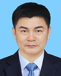
Tingyu Lin
Mark Huang
CTO & VP
A-kelon (Huizhou) Optronics
"Advanced Packaging Innovation Challenges - Super-thin Optical SiP & CIS"
"先进的封装创新所面临的挑战 – 超薄光学SiP和CIS"
Mark Huang
A-kelon (Huizhou) Optronics Ltd, China

The market demand for ultra-thin portable electronic products like smartphones and mini-tablets continues to grow. Consumers want smaller devices and longer battery life which is driving the development of several new types of advanced packaging for further size reductions.

Even image-capturing devices based upon CMOS image sensors (CIS), need to thin down. As an example of the innovation in packaging that is being demanded, a novel manufacturing method using rigid-flex printed circuit board (R-F PCB) combined with flip-chip bonding for ultra-thin CIS modules will be described. This new technology is targeted to reduce the CIS module by up to 0.4 mm in thickness as compared with today’s widely used chip-on-board (COB) module.

This new process flow contains many process modules recently developed combined with non-traditional “packaging” steps. The CIS module process includes physical vapor deposition (PVD) of Cu-Ti seed layer, photolithography together with wafer-level plating to form copper pillar bumps, metal etch after photoresist stripping, wafer thinning, dicing, flip-chip bonding followed by underfilling, IR glass bonding, RLC surface mounting, and reliability test. Clearly this is not ordinary packaging run on a traditional packaging “line”.

Many other functional areas, which are often overlooked in packaging development, need to be incorporated for successful advanced technology. The importance of cleaning and test will be highlighted in the development of Super-thin Optical SiP & CIS packages.

移动电话和平板电脑等超薄便携式电子产品的市场需求,消费者对更小的电子产品和更长的电池寿命的需求驱动了各种先进封装技术的发展

包括CMOS图像传感器(CIS)在内的图像捕捉设备需要进一步降低厚度。在这篇演讲中介绍了在封装技术中的一个创新案例,一种使用软硬结合线路板(R-F PCB)和Flip-Chip Bonding相结合来实现超薄CIS模组新的制造方法。和现有的普遍使用的COB(Chip-on-Board)技术相比,此项新技术可进一步使CIS模组的厚度减少到0.4毫米。

此新工艺流程采用了很多现有模组的封装技术,同时也采用了非传统的【封装】步骤。CIS模组流程包括了,Cu-Ti种子晶层的物理气相沉积(PVD)、光刻与晶片级电镀以形成铜柱凸块、光阻剥离后的金属蚀刻、晶片减薄、切割、倒装键合、然后是,底部填充、IR玻璃键合,RLC表面贴片和可靠性试验。很明显,以上步骤并非一个标准的封装线的封装流程。

为实现优秀的先进技术,在封装工艺流程中经常被忽视的很多其他功能部分也需要关注,例如,清洗和测试在超薄光学SiP和CIS封装的开发中也起着重要的作用。

Biography(English)

Mark Huang

Mark Huang holds a Ph.D. degree in Polymer Chemistry from The Institute of Chemistry, Chinese Academy of Science. And was a Postdoctoral Fellow at National University of Singapore. Following his studies, he has held senior material and process engineering roles at Yizheng Chemical Fiber Company, Hitachi Chemical Asia/Pacific, Micron Semiconductor Asia, StatschipPAC, and the Institute of Microelectronics. In 2011 he was the Director of Technology Development at SFS Group-Unisteel Technology Group Company. Dr. Huang then became the CTO in charge of thru-silicon via (TSV) fabrication at Speed Wireless Technology in 2014. He recently joined A-Kelon Optronic Ltd as CTO & VP leading technology development for CMOS Image Sensor (CIS) Wafer-level Packaging (WLP) and finger print sensor (FPS) packaging.

His in-depth expertise in IC packaging materials (underfill, encapsulants, die-attach film/paste etc) has enabled him to be a key technical contributor to the R & D and implementation of advanced assembly technologies including Flip Chip in Package (FCIP), System in Packaging / Multi Chip Package (SiP/MCP), Wafer Level Chip Scale Package (WLCSP), Cu-Pillar Interconnection, Through Silicon Via (TSV), Ultra-thin Wafer Processing and other cost-viable packaging solutions. He has published over 50 technical papers and holds 50 U.S. patents and 1 Singapore patent. His research interests include 3D-IC integration, TSV fabrication and assembly, as well as semiconductor packaging materials.

Dr. Huang was honored as a "Plan 1000" expert by China’s Global Expert Recruitment Program in 2016.

Biography (Chinese)

黄双武

黄双武博士,第12批国家千人计划特聘专家,中国科学院化学研究所高分子化学博士(1996)加坡国立大学博士后(1996-1998), 在新加坡和美国工作18年,先后服务于日立化成(HCAP)任高级工程师,美光科技(Micron)任主任研究员,星科金朋( StatschipPAC)任高级经理,新加坡微电子研究所(IME)任技术顾问,瑞士SFS集团旗下Unisteel公司技术总监。 2014回国加入硕贝德(Speed)任CTO负责TSV制造和指纹模组封装技术开发,先就职于凯珑光电(A-Kelon) 任CTO和VP负责CIS WLP和指纹传感器(FPS)封装的技术开发。黄博士擅长于IC封装材料(底部填充、封装剂、贴模薄膜/浆料,晶圆清洗等), 并一直致力于先进组装技术的研发与实施,包括封装倒装芯片(FCIP)、封装系统/多芯片封装(SiP/MCP)、晶片。水平芯片规模封装( WLCSP),铜柱互连,通过硅通道(TSV),超薄晶片处理和成本可行的封装解决方案。共发表论文50余篇,持有美国专利50项, 新加坡专利1项,中国发明专利3项,实用新型专利29项。他的研究兴趣包括3D-IC集成、TSV制造和装配以及创新材料的开发与应用

> alt="Link to Keynote at Suzhou">
9:15 - 10:00
Shenzhen
Keynote Address
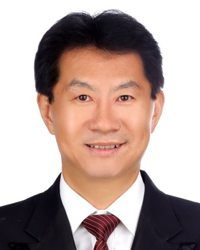
Tingyu Lin
Tingyu Lin
Technical Director
National Centre for Advanced Packaging (NCAP), China
Large Panel Fan-Out (LPFO) Technology Overview and Development
大板扇出技术综述及研发
Tingyu Lin
National Centre for Advanced Packaging (NCAP), China

Fan-out Wafer Level Packaging (FoWLP) technology is being rapidly adopted due to improved electrical-thermal performance, higher levels of integration, and great flexibility all at lower costs than traditional semiconductor packaging. This is possible due to highly-efficient wafer based processes and equipment. Large Panel Fan-Out (LPFO) promises further cost reductions while providing significantly larger volumes to meet the growing demand. Beyond simply increasing the substrate from a wafer to a panel, there are many challenges in developing and commercializing LPFO which will be discussed.

The National Centre of Advanced Packaging (NCAP) China led a development consortium in China which has conducted extensive process and reliability assessments for LPFO. In the current Stage 2 activities, NCAP will launch a consortium for System-in-Package (SiP) fan-out and will build engineering lines with Guang Dong Industrial University in FoShan city. Stage 1 results, planning for Stage 2, and remaining commercialization challenges will be presented.

大板扇出技术由于高效,低成本,出众的功能,高度集成及灵活性,这几年越来越得到人们的关注。 华进半导体基于第一阶段的国际联合体的工艺及可靠性开发及评估,取得了很大成绩。 华进半导体在联合体第二阶段联合广东工业大学国家重点实验室共同打造国内第一条大板扇出工艺线。 这个报告重点谈到华进第一阶段的研发成果及第二阶段的在广东佛山建造的大板扇出工艺线的规划。

Biography (English)

Tingyu Lin

Dr. Tingyu Lin has more than twenty years of experience in design, process, assembly, reliability and equipment development in electronics packaging, semiconductor, consumer electronics, PCBA, thermal and aerospace industry.  He received a B.E. degree in thermal engineering from Tsing Hua University and a M.E degree in aerospace engineering from the Ministry of Aerospace in 1990 in China and a Ph.D in microelectronics from National University of Singapore (NUS) in 1997. He is a Motorola (Google) certified Six Sigma Black Belt in 2012. From 2013 to present, he has been a technical Director of the National Centre for Advanced Packaging (NCAP), China. He is responsible for strategy planning, organizing consortium, and leading R&D activities on advanced packaging material and equipment for the development and commercialization of fan out, TSV, and 2.5D process solutions.  From 2012-2013 he was a program director of the Institute of Microelectronics, Singapore (IME), and responsible for 2.5D, fan-out, and WLP development. From 1997-2012 he worked as a senior manager in Philips, Lucent Technologies (previously AT&T Bell Lab) and Motorola Electronics. where he was responsible for consumer electronics design, process and product development, and advanced manufacturing in advanced IC packaging in flip chip module and SiP, and supply chain management and mobile product quality and reliability improvement.  He has been engaged in more than 100 product design & process development in mobile module, IC component, and consumer electronics, etc.  Dr. Lin had published 150 papers and filed more than 10 patents. In addition to receiving many excellent paper awards and providing keynote talks at several conferences, he drove and passed two international ASTM sputtering material standards(F3166 & F3192)for TSV development. He received several Motorola Innovation awards in 2008。

Biography (Chinese)

林挺宇

  • 中国清华大学(BS);新加坡国立大学 (Ph.D); 阿德莱德大学(MBA)
  • 2014年国家“千人计划”入选者
  • 获得摩托罗拉认证的6Sigma质量黑带,发表论文百余篇,国际专利数十项
  • 先后任职于飞利浦、朗讯、摩托罗拉、新加坡微电子所,目前任职于华进半导体封装先导技术研发中心有限公司,担任技术总监(扇出型封装工艺、材料、可靠性与失效分析方向)、战略研究与产业化部长
> alt="Link to Keynote at Suzhou">
10:00 - 10:30
Session 1
Market Report
An overview of the test consumables market:
"Strong Global Demand for Semiconductors Brings Unlimited Opportunities in China"
"半导体芯片性能和寿命测试插座的中国市场"
Lin Fu
VLSI Research
Abstract and Biography (English)

Semiconductor sales have almost doubled since the financial crisis with revenues exceeding $422Bn in 2017. Last year was not only a good year but also a very profitable year for the industry. 2018 is shaping up to be another favourable year and under this positive environment, global sales of test and burn-in sockets are expected to grow strongly. This presentation explains what is happening in the short-term and reviews the current long-term drivers for the test and burn-in socket market. This overview is followed by a preliminary analysis which examines the Asian test and burn-in socket market with the main focus on how the Chinese market is expected to develop over the next 5 years.

Lin Fu received the Bachelor Degree in Electrical and Electronic Engineering with first class honours from Edinburgh University in 2013. Then, she started her postgraduate study in Cambridge University. In the meantime, she published more than ten papers as the first author or co-author in the IEEE Transactions on Applied Superconductivity, Superconductor Science and Technology, Applied Physics Letters and so on. In 2018, she received the doctoral degree in Engineering from Cambridge University and started to work in VLSI Research Europe. At present, she focuses on the marketing research and analysis related to semiconductor test consumables, including probe cards, test and burn-in sockets and device interface boards.

Abstract and Biography (Chinese)

2017年全球半导体行业收入超过4,220亿美元,大约两倍于经济危机时的行业收入。2017年不仅是收益颇丰的一年,同时半导体市场也收获了高额利润。在利好的行业趋势下,2018年测试座及老化座的销售额有望增长强劲。此次演讲将阐述测试座及老化座的市场现状,长期驱动因素,以及未来五年亚洲市场尤其是中国市场的前景分析。

Lin Fu
付琳于2013年毕业于爱丁堡大学,并获得电气与电子工程一等荣誉学士学位。同年,在剑桥大学继续研究生学习。期间,她作为第一作者或合作者在国际期刊及会议上发表论文十余篇。2017年,付琳取得剑桥大学工学博士学位并开始在VLSI Research Europe工作。目前,她致力于半导体测试领域的市场研究与分析,包括探针卡,测试插座及设备接口板等。

> alt="MarketPlace">
10:30 - 10:45
Break

Enjoy time to meet with the presenters and network while refreshments are served.

10:45 - 12:15
Session 2
5G and mm-wave Test Challenges
High frequency challenges for next generation applications
Regional and global experts will share their expertise and solutions to the challenges of high frequency / speed and radio frequency (RF) test.

Technical presentations in English or Mandarin. Slides in English with bilingual question & answer period.

"RF Module Test Challenges"
"射频模组的测试挑战"
Keith Schaub
Advantest
Roger McAleenan
Advantest
Ira Leventhal
Advantest
Abstract and Biography (English)

5G mm-Wave (i.e. 28GHz and above) brings completely new test challenges never before faced in production radio frequency (RF) integrated circuit (IC) automated test equipment (ATE) environment. Channel bandwidths above 1 GHz are already challenging, but the reduced wavelength will make antenna on chip (AOC) and antenna in package (AIP) a reality for the production test environment. Up to 256 antenna arrays will “be the package”. In many cases, over-the-air (OTA) testing will be the only objective solution. Some of the key challenges that will be discussed in this presentation are:

  1. Antenna impedance changes the power amplifier (PA) efficiency, so what we tested pre- package may not hold true once the antenna is attached.
  2. Receiver sensitivity is subject to thermal changes. With the antenna embedded as part of the package, as the IC heats/cools, the noise sensitivity changes – somehow this will need to be tested and verified.
  3. No standard connectors are available. Historical mm-Wave has a standard connector to verify functionality or performance. This just isn’t practical, probably not even possible. Meaning, passive measurements won’t be possible.

Keith Schaub Keith Schaub is currently Vice President of Business Development at Advantest America, Inc. He has over 20 years of experience in Semiconductor Test, with special focus on RF and System-on-a-Chip test. Keith has worked on the design and development of multiple generations of ATE systems at Hewlett-Packard, Agilent Technologies, and Advantest, and holds patents in a variety of test-related technologies. He is the founder of several startups, including Wireless SOC Test, Inc., and author of the book “Production Testing of RF and SOC Devices for Wireless Communications”. Additionally, he has authored several papers and editorials on the state of RF/wireless SOC/SIP testing and market trends, for numerous industry publications including Evaluation Engineering and Test and Measurement World. Keith holds a BSEE degree from Texas A&M University and an MSEE degree from the University of Texas at Dallas.

Abstract and Biography (Chinese)

5G毫米波(即,28 GHz以上)使射频(RF)集成电路自动化测试设备(ATE)带来前所未有的全新挑 战。1 GHz以上的信道带宽是非常具有挑战性的,但是减小的波长将使片上天线(AOC) 和天线封装(AIP)使规模化生产测试成为现实。多达256个天线阵列将被封装在一起。在 许多情况下,无线(OTA)测试将是唯一的客观解决方案。本次报告将讨论的一些关键挑 战是:

  • 1.天线阻抗改变了功率放大器(PA)效率,所以我们在预封装前测试的结果在加装了天 线后并不一定是对的。
  • 2.接收灵敏度受温度变化影响。随着天线作为封装的一部分嵌入,随着IC加热/冷却,噪 声灵敏度会随着改变,这将需要测试和验证。
  • 3.没有标准连接器。历史毫米波有一个标准连接器,以验证功能或性能。但是这是不实 际的,甚至不可能,也没有意义,无源测试是不可能的。

Keith Schaub
基思.肖布先生目前是美国爱德万公司业务开发部门副总裁。他拥有超过20年的半导体测试经验,特别专注于射频和片上系统测试。基思曾在惠普、安捷伦科技和爱德万测试公司等多家ATE测试公司任职并设计和开发了多代ATE测试系统,并拥有各种测试相关技术中的多种专利。他是多家初创公司的创始人,其中包括无线SoC测试公司,以及“无线和SOC芯片的无线通信量产测试”一书的作者。此外,他还撰写了多篇关于RF /无线SoC/SIP测试和市场趋势的论文和社论,包括工程评估和测试以及测量世界在内的众多行业出版物。基思拥有德克萨斯农机大学的电子工程学士学位和德克萨斯大学的电子工程硕士学位。

> alt="Session 2.1">
"Over the Air Test for Antenna in Package IC"
"片上级天线封装芯片的无线测试"
Dongmei Han
Xcerra
Abstract and Biography (English)

As 5G wireless technology is being developed, cell phone makers are turning to Antenna in Package (AiP) integrated circuits (ICs). AiP is a new trend in IC packaging which makes smaller ICs with higher levels of integration that adds an antenna to the IC(s) inside the package. Antenna in Package allows integration of all the complex RF components, together with the base-band circuitry into a complete self-contained module that greatly facilitates the work of the system integrator. As the customer demand increases for higher performance products, available area for system modules is getting smaller and smaller. AIP design means a system integrator no longer needs to design complex RF circuits at the application PCB level and reduces the overall size of the complete application.

How to test those AIP ICs becomes a new and hot topic. This paper will present how we implement OTA test in our test system. Since 5G frequency is getting into 60GHz, our system also involves mmWave solutions.

DongMei Han is a Signal Integrity Project Manager/Engineer with Xcerra Corporation. She is currently working on over the air mmWave test sockets with a bandwidth of over 100 GHz. DongMei holds a Master of Engineering degree for the University of Illinois. DongMei started her career with Motorola in the Cellular Subscriber Division where she worked as an Analyzer Engineer and Team Leader. DongMei later joined the Tyco Safety Products group in Canada where her work included system and board level RF design and test, including transmitters, receivers used for ISM band applications. This work included RF and analog circuitry including filters, amplifiers, switches, LNAs, PCB antennas, PLLs, VCOs, AGC, and matching network. Before joining Xcerra, DongMei was involved with RF antenna theory, electromagnetic modeling, and energy harvesting devices, along with wireless sensors, and wireless systems architectures.

Abstract and Biography (Chinese)

随着5G无线技术的发展,手机制造商正在转向天线封装(AiP)集成电路(IC)。 AiP是IC封装的一个新趋势,它使具有更高集成度的小型IC为封装内的IC增加了天线。 天线封装允许将所有复杂的RF组件与基带电路集成到一个完整的独立模块中,极大地方便了系统集成商的工作。随着客户对更高性能产品的需求增加,系统模块的可用面积越来越小。 AIP设计意味着系统集成商不再需要在应用PCB级别设计复杂的RF电路,并减少整个应用的整体尺寸。

如何测试这些AIP IC是一项新的挑战,也是测试中的“热门话题”。本演示文稿详细介绍了我们如何在测试系统中实施无线(OTA)测试。由于5G计划用于60GHz左右的频率,因此这些解决方案必须适应mm波段的工作。

DongMei Han
韩冬梅是Xcerra公司的信号完整项目经理/工程师。她目前正在研究超宽带宽度为100GHz的mmWave测试插座。 冬梅拥有伊利诺伊大学工程学硕士学位。冬梅在摩托罗拉开始了她的职业生涯,在蜂窝用户部门担任分析工程师和团队负责人。 冬梅后来加入了加拿大的Tyco安全产品集团,她的工作包括系统和板级RF设计和测试,包括用于ISM频段应用的发射机,接收机。 这项工作包括RF和模拟电路,包括滤波器,放大器,开关,LNA,PCB天线,PLL,VCO,AGC和匹配网络。 在加入Xcerra之前, 冬梅还参与了射频天线理论,电磁建模和能量采集设备,无线传感器和无线系统架构

> alt="Session 2.2">
"Feasibility Evaluation of a Spring Pin Wafer Probing Approach for a 5G WLCSP Application"
"弹簧探针在5G晶元级别的测试应用可行性研究"
Jose Moreira
Advantest
Krzysztof Dabrowiecki
Feinmetall
Paul Hurst
Harbor Electronics
Thomas Gneiting
Admos
Ali Abdallah
Admos
Abstract and Biography (English)

In this presentation, we will show a simulation based study that evaluates the feasibility of using a spring pin based wafer probing approach to test a wafer level chip scale package (WLCSP) integrated circuit (IC) for a 5G application. The target frequency is 28 GHz which presents significant design challenges for the probe card printed circuit board (PCB) and the probe head design. The target device under test (DUT) is a WLCSP IC with a non-regular ball grid array (BGA) and a pitch of less than 0.4 mm between the radio frequency (RF) signal pins and ground (GND) pins. For mm-wave frequencies it is critical that the probe card PCB and the probe head are co-designed together at the same time and simulated together with full 3D electro-magnetic (EM) simulation. A close relationship with the automated test equipment (ATE) system is also critical since at the end the measurement performance will be defined by the entire system. Although there are proven wafer probing technologies for mm-wave applications (e.g. membrane based probe cards), a spring pin based probing solution would provide a significant advantage for a high volume, low cost test strategy. Therefore, it is important to understand what trade- offs there are between using spring pin and other technologies for 5G application in high volume testing. In this presentation, we will discuss the design challenges and present some of the trade-offs that need to be evaluated for a spring pin based probing solution for mm-wave 5G applications.

Jose Moreira received a Licenciatura and M.S. degrees in Electrical and Computer engineering from the Instituto Superior Tecnico of the University of Lisbon. He was with Agilent Technologies and its spin-off Verigy since 2001 which was later acquired by Advantest. He is currently a senior R&D staff engineer at Advantest Germany. His research interests are signal and power integrity, multigigabit interfaces characterization and test fixture design and measurement. He is co-author of the book “An Engineer’s guide to Automated testing of High-Speed Interfaces”.

Krzysztof Dabrowiecki is the Product Manager at Feinmetall, Germany. He is responsible for development of probe card solutions for flip chip and WLCSP test applications. He is an author of numerous presentations, patents and published articles in the areas of probe cards in the US and Germany. Kris holds a Master’s degree in Mechanical Engineering from Gdansk University of Technology (GUT). He is a member of ASME and IEEE.

Abstract and Biography (Chinese)

在本演示中,我们将展示一项用来评估使用弹簧卡印刷电路板(PCB)和探头设计的可行性的仿真策略。

被测目标器件(DUT)采用非规则球栅阵列(BGA),是一种晶圆级芯片尺寸封装(WLCSP)的集成电路。基于晶圆探针方法测试WLCSP的5G应用芯片,芯片射频用引脚的间距小于0.4mm。

目标频率为可以展现RF针卡与地的重要设计挑战的28Ghz频率。

对于毫米波频率,探针卡PCB和探针头同时设计和基于3D电磁(EM)仿真技术同时仿真是至关重要的,与自动测试设备(ATE)系统的密切关系也非常关键,因为最终测量性能将由整个系统定义。

虽然已经有成熟的晶圆探测技术用于毫米波应用(例如基于膜的探针卡),但基于弹簧针的探测解决方案将为大批量,低成本的测试策略提供显着的优势。因此,重要的是要了解在大批量测试中使用弹簧销和其他技术进行5G应用之间的权衡。在本演示中,我们将讨论设计挑战并介绍一些需要针对mm-wave 5G应用的基于弹簧引脚的探测解决方案进行评估的权衡。

Jose Moreira
毕业于里斯本技术大学电气和计算机工程系,获得理科硕士学位. 他目前担任Advantest德国公司的高级工程师。 从2001年, 他曾在Agilent Technologies的测试部Verigy工作, 后该测试部被Advantest收购。 他的研究领域包括信号和功率完整性,高频(千兆级)连接界面特性和测试制具, 他还是Artech House 出版的《测试高速接口自动化测试设 备【Testing High‐Speed Interfaces with Automated Test Equipment】》一书的联合署名作者。

Krzysztof Dabrowiecki
是德国Feinmetall的产品经理. 他负责为倒装芯片(覆晶技术)和WLCSP测试应用开发探针卡(探针板)的解决方案. 他在美国和德国的探针卡(探针板)领域发表了大量简报,专利和论文. Kris拥有Gdansk(格但斯克)理工大学机械工程硕士学位. 他是ASM(美国机械工程师协会)和IEE(电气与电子工程师协会)的成员.

> alt="Session 2.3">
12:15 - 13:30
Lunch &
TestConX EXPO
TestConX EXPO
opens at 12:15
Enjoy the delicious hot buffet lunch and networking time. Then take the time to explore the TestConX EXPO. There will be many great exhibits to connect electronic test professionals to solutions. You will be certain to see something new or meet someone new.

As attendees to TestConX know, there is always excellent food, drinks, and time for attendees to network with exhibitors!

TestConX EXPO will open at 12:15 and will remain open throughout the afternoon until 18:00

13:30 - 15:00
Session 3
High Frequency and High Current
Latest presentations on challenges of High Frequency and High Current
Regional and global experts will share their expertise and solutions to the challenges of testing high frequency and high current applications.

Technical presentations in Chinese or English as noted. Slides in English with bilingual question & answer period.

"Interpretation and Application of Test Contactor Specification"
"测试接触器规范的解释与应用"
Bert Brost
Xcerra Corporation
Abstract and Biography (English)

This presentation describes and defines the data used to specify contactors and test sockets, and probe heads for test. The source methodology and process for developing the lab data describing these performance specifications is reviewed. In addition, the interpretation of data describing the performance of Over-the-Air contactors via antenna gain, bandwidth, and radiation pattern is covered along with statistically predicting field performance of the test probe versus performance measured in a test lab. By covering the technology fundamentals, this presentation is generic to probe technology in general and not just one specific type of probe.

Presented will be lab data describing the performance of several mainstream probe architectures for contacting Wafer Level Chip Scale Packages (WLCSP). And this presentation will create a common understanding of how to read, interpret, and communicate data for selecting the right probe technology for WLCSP test applications.

This presentation goes beyond just the probes and speaks to other factors that contribute to the overall performance of the contactors, test sockets, and probe heads for test. For example, the probe head housing design and materials used are important aspects that need to be understood for optimized performance. The success of the data-driven probe selection approach is reliant upon the quality of the supplier provided data. Therefore, this presentation will describe the reports typically provided using WLCSP Metrology reports as an example.

Bert Brost is a Senior Product Manager for Xcerra Corporation. With more than 35 years of experience in backend test, Bert has held senior management positions with Johnstech International and Control Data Corporation. Bert started his career in engineering with Micro Component Technology (MCT) designing test electronics and later worked as an engineer for Sick Optik Elektronic GmbH. Bert holds several undergraduate degrees and a MBA from the University of St. Thomas, Minnesota.

Abstract and Biography (Chinese)

本文的目的是描述和定义用于指定接触器和测试插座的数据,以及用于测试的探头。这包 括开发用于描述接触器、测试插座和探头的性能的实验室数据的来源方法方法和过程。

在此基础上,本文将介绍描述天线增益、带宽和辐射模式描述的空中接触器性能的数据, 以及在测试实验室中合格的测试探针的统计预测场性能。

由于本文是纯粹的技术性质,以及通用的探测技术,可是它不会说任何类型的探头。

介绍了描述晶圆级芯片级封装(WLCSP)的几种主流探针结构性能的实验室数据。本文 的目的是创建一个共同的理解如何读取,解释和沟通数据,选择正确的探针技术为 WLCSP测试应用程序。

该文件超出了探头,并谈到其他因素,有助于整体性能的接触器,测试插座,探头测试。 例如,探头头壳体设计和材料是需要被理解的重要方面,以优化性能。数据驱动的探针选 择方法的成功依赖于供应商数据的质量。本文将描述所提供的报告,包括WLCSP计量报 告。

伯特先生是XCERA公司的高级产品经理。拥有超过35年的后端测试经验,伯特先生曾与Johnstech和Control Data Corporation担任高级管理职位。 伯特先生最初任职于微电子技术(MCT)公司从事设计电子电路,后来他成为了Sick Optik Elektronic 公司一名工程师。他在德克萨斯圣托马斯大学明尼苏达分校拥有数个本科学位和一个工商管理硕士学位。

> alt="Session 3.1">
"One Type Wiping Contact Introduction"
"一种刮擦接触方式的介绍"
Xiaofei “Shaffer” Ji
Smiths Interconnect
Abstract and Biography (English)

Wiping contact is widely used for lead less peripheral IC packages such as QFN which pad surface usually is covered by an oxidation layer or sometime even with some contaminations. The oxidation layer is very thin but hard wearing and insulated. By high strength base material and noble metal coatings, the wiping contact is tended to displace surface contaminants and pierce through the insulated oxidation layer. The effectiveness of wiping action is dependent on normal load, contact geometry, surface material, nature of pad contamination, and distance of wiping. It is generally known from field experience that even gold-plated contacts need wiping in order to get a reliable contact.

Wiping contact can get significant advantages in compliance, tri-temperature handling and current carrying capacities by a specified signal path & related material. Wiping contact secures to socket using an elastomer. The compliance structure has built in the wiping contact without any influence of the elastomer. Current carrying capacity is decided by the contact shape, material, thickness & housing feature design. This contact structure enables high current and higher temperature test capability. By a rigid design of the contactors, it can support up -1dB insertion loss at 10GHz bandwidth. Minimal impact on PCB & package pad, easy to clean and maintenance are other advantages. Besides, it also enables a longer life span comparable to the spring probe.

Xiaofei “Shaffer” Ji is currently the Mechanical engineer of Smiths Interconnect Suzhou site. He graduated from Southern Yangtze University in 2010, majored in Mechanical Design & Automation. Now his major work is designing and developing some contact pins。

Abstract and Biography (Chinese)

刮擦式接触是一种广泛用于扁平无引脚芯片(QFN)的测试方案,通常芯片的引脚比较容易氧化 或者被其他物质污染,特别是氧化膜层很薄,很难去除。对于高强度材料和贵金属镀层来说,刮 擦式接触可以去除环境污染物和氧化膜层。刮擦效果取决于载荷、几何特征和接触表面材料、污 染物特性以及刮擦距离。业内通常认为,即使是金镀层,接触刮擦也可以提高可靠性。

刮擦式测试方案在服从性,温度适应性和载流量上有着显著的优势,因为它采用指定信号路径的 方式。刮擦式方案使用弹性橡胶体镶嵌在插座内部,但是不会对插座行程产生影响。探针的形状 ,材料,厚度以及内部设计决定了更高的载流量和温度适应性。刮擦式可以支持-1dB最高10 GHz 的带宽。而刮擦式接触对PCB和Package的pad影响非常小,所以也方便了后期的清洁和维护。 除此之外,刮擦式测试有着更长的使用寿命。

Xiaofei “Shaffer” Ji
吉小飞现在是Smiths Interconnect苏州公司的机械设计工程师,他在2010年毕业于江南大学机械设计及其自动化专业。目前他主要从事于接触探针的设计和研究。

> alt="Session 3.2">
"Contact Probe CCC Study and Application"
"接触探针的电流载荷能力的研究和应用"
Tomohiro Yoneda
NHK Spring Co., Ltd
Terry Wang
Infineon
Hongzhen Zhao
Testpro Pte. Ltd
Abstract and Biography (English)

Semiconductor industry is moving towards producing smaller packages, but more functions, faster response and higher power. As such, the contact development towards using contact pins with high test capability and stability for testing is inevitable.

During the contact pin selection and socket design, a designer generally need take into consideration on six factors: electrical, mechanical, thermal, lifespan, lead time and cost. Among all six factors, electrical aspect is deeming of most important parameter for the automotive microcontroller and power products testing. among electrical parameters, Current Carrying Capability (CCC) is the most important factor that influences the test capability and stability of contact pins. Although there are some previous studies that addressed the contact pins CCC every year, but the test environment and requirements is not fully applicable. Each semiconductor companies have their own specialized fields; test requirements are drastically different. Some contact pin suppliers provide CCC as per International SEMATECH Manufacturing Initiative (ISMI) standard method; while some are not.

This study is a collaboration between Infineon and Nippon Spring Co. (NHK), based on the newly- developed contact pin. The aim of the study is to explore the CCC effect and difference on CCC readings, based on the 2 variables. One is traditional ISMI standard force-dependent while the other is temperature-dependent. The readings were obtained respectively. The analysis deduced that there is near 50% difference in CCC between the two methods.

High temperatures, such as 150°C, pose another challenge to the productive testing. When the pin temperature rises further, e.g.: 150°C level, the pad or lead Tin plating layer tend to be soften. As a result, it complicates contact behavior between pin and lead/pad. A ~25% reduction in CCC was observed at 150°C in comparison to ambient environment.

Generally, the tip style of contact pins does not affect CCC readings too much. Instead, the pin structure and feature dimension play more significant role. Regression statistics in the analysis can enable users to quickly validate the CCC specification from various sources. In addition, it’s to enable users to make a rough estimation of the CCC range for a new contact pin.

With the study, the CCC specification from contact pins suppliers will be better understood and applied. With the study, a clearer picture of CCC will be shown to the socket designers and the engineering users.

Tomohiro Yoneda is the project manager of NHK Spring Co., Ltd. He graduated from Kyushu Institute of Technology with Bachelor Degree of Mechanical Engineering in 2008.

Yoneda has 10 years of experience in the field of contactor designing from socket, probe head, driver IC to LCD test unit. He has led the design team for overall test socket, probe head, pogo pin development, design and engineering for 3 years.

With his rich knowledge in test contactors, his current focus is on the development of high current and RF solution for automotive IC testing.

Abstract and Biography (Chinese)

伴随着半导体测试科技的飞速发展,市场上的测试产品尺寸越来越小但是芯片的功能,速度和 功耗却一直在不断增加,因此,目前测试开发的趋势是如何实现测试探针满足不断提高的测试 要求和测试稳定性。

在选择测试插座和探针设计时,我们通常会考虑六个主要因素,分别是探针的电气,机械,热 性能,使用寿命,交付时间和成本。在这六个因素中,电气指标被认为是测试的最重要参数。 虽然现有一些有关电流承载能力的研究,但是其应用领域各不相同,每个公司都有自己的侧重 点和不同的测试要求。探针供应商对电流承载能力的测试方式也不尽相同。

此次的研究是英飞凌和日本发条株式会社共同合作进行的。该研究的目的是基于两个变量去探 索电流承载能力的差异。一种是基于传统ISMI标准的弹簧力衰减测量法,另一种是基于温度攀 升的测量法。从两种的测量读数结果我们可以大概推断这两种测量法之间的差异可高达50%。

在高温测试中我们对探针的耐高温性能提出了另一个挑战,当探针的温度不断攀升,例如150 摄氏度,这时候产品的镀层趋于软化造成镀层易损,在150度下探针的电流承载能力比常温下 明显降低。

研究发现,探针的测试头形状设计通常不会显著影响电流承载能力,是探针本身的设计结构和 尺寸起着主要的作用。此研究得到的数据能帮助用户快速验证电流承载能力的范围,此外,客 户还能从中快速估算出同类型但是不同尺寸探针的电流承载能力范围。

这次研究有利于我们更好地理解和应用探针,使得插座设计师和测试工程师对电流承载能力的 概念更清晰。

Tomohiro Yoneda

米田知広于2008年毕业于日本九州工业大学获得机械工程学士学位,他现在就任日本发条株式 会社的项目经理。

米田拥有十年测试插座,探针,探头的设计和开发经验。凭着这些丰富的经验,他现在带领日 本发条株式会社设计和开发团队,致力于研发高电流和高频高速的探针解决方案。

> alt="Session 3.3">
15:00 - 15:30
Networking Break
TestConX EXPO Continues

Enjoy additional time to meet with the presenters, network, and explore the TestConX EXPO further. There will be many great exhibits to connect electronic test professionals to solutions.

15:30 - 17:00
Session 4
Advanced Contact & Socket Technology
Latest presentations on challenges of Advanced Contact & Socket Technology
Regional and global experts will share their expertise in advanced contact and socket technology.

Technical presentations in Chinese or English as noted. Slides in English with bilingual question & answer period.

"The Impact on Probe Pin Performance of Different Plunger Cutting Methods at Device Side"
"冠装探针的粗糙面对探针性能的影响"
SL Wee
Test Tooling Solutions Group
Alfred Lim
Test Tooling Solutions Group
Takuto Yoshida
Test Tooling Solutions Group
Abstract and Biography (English)

A key concern for ball grid array (BGA) packaged semiconductor device testing is whether the contact resistance (CRES) of probe pins is low and stable during test. A high and inconsistent CRES before and during test will result in higher solder migration and down time for cleaning. This presentation will examine the impact of the manufacturing process on the probe pin performance.

Lead-free solder balls used for BGA devices can easily cause solder migration to the device side plunger (Plunger ‘A’) of a spring probe pin. The migrated solder, if not cleaned thoroughly and timely, will oxidize on the pin tip surface area and cause high contact resistance during test. The key is to minimize the CRES and the solder migration; thus reducing the down time for cleaning and the throughput of the test operation.

The purpose of this investigation is to establish the link between the different cutting methods to produce a pin and the performance of the pin in term of CRES and solder migration. Specifically, what is the impact of the roughness of the cut surface on the CRES and solder migration of a probe pin?

Various Plunger A of the same design, but of different degree of roughness and finishing, will be produced using 3 different cutting methods and tooling. Apart from the Plunger A, the pins are assembled using the same parts from the same production lot. These pins are mounted in the same cycling jig to conduct the CRES and solder migration experiment. To accelerate the solder migration, a high current is passed during the touch down with the solder plate. Measurement and observation of the CRES and solder migration are taken at intervals. Evaluation and conclusion will be made on the study of the data collected.

SL Wee received his MBA from the California State Polytechnic University, Pomona and his BSc from the University of Southern California. He joined Test Tooling Solutions Group as its Chief Executive Officer in 2006. Prior to that, he has held various leadership and management positions in GE Capital, CIT and OCBC Bank.

Abstract and Biography (Chinese)

半导体球栅阵列(BGA)封装测试中的一个关键问题是探针的接触电阻在测试过程中是否稳 定。在测试之前和测试期间的超高和不稳定的接触电阻会导致更高的合金和清洁频率, 本论 文将探讨制造工艺对探针性能的影响。

用于BGA封装的无铅焊料球可以容易和弹簧探针的顶部(顶针A)产生合金,如果不彻底和 及时清洗,会在针尖表面区域形成氧化膜,并在测试过程中引起超高的接触电阻。其中主要 的关键是如何减小接触电阻和合金,从而减少清洁的频率和提高测试产量。

本研究的目的是建立不同的切割方法之间的对应关系,来解释探针在低接触电阻和合金方面 的性能。具体地说,切割表面粗糙度对探针的接触电阻和合金的影响。

我们采用同款设计, 但以3种不同的切削方法和刀具,产出不同粗糙度和精整度的顶针A。除 了顶针A外,套筒用同一生产批次的相同部件组装。这些探针安装在相同的循环夹具进行接 触电阻和合金实验。过程中通过高电流来加速合金情况在固定的间隔周期内, 测量和观察接 触电阻和合金, 对收集的数据进行评价和总结。

SL Wee 毕业于美国南加州大学并获得大学理科学士学位,之后更取得加州州立大学之企业管理硕士学位。 2006年,他以首席执行官的身分,加入Test Tooling Solutions Group。 在此之前,他于GE capital、CIT集团与华侨银行皆有相当丰富的领导与管理经验。

> alt="Session 4.1">
"Test yield control by on-line laser cleaning"
"通过在线激光清洁来控制测试良率"
J.M. Lee
IMT Co. Ltd.
J.W. Lee
IMT Co. Ltd.
Abstract and Biography (English)

A laser cleaning process will be described that has been successfully applied to remove the surface contamination from socket pins that have become “dirty”. The contamination on the pin surface is mainly the tin (Sn) based lead frame and ball material which is very strongly adhered and negatively impacts test yield. The laser cleaning can be applied for cleaning of test sockets where diverse pin shapes and materials are employed. In order to evaluate the cleaning performance, the surface morphology was investigated by microscope and scanning electron microscope (SEM). The electrical contact resistance was also measured before and after cleaning. It was found that the laser cleaning was very effective in removing the surface contamination on different types of sockets. And the improvement of contact resistance after laser cleaning is significant enough to make reuse of pins practical to provide a longer lifetime. It was also found that a significant increase in first test yield and higher levels of yield control could be obtained by on-line laser cleaning.

J. M. Lee J. M. Lee is CTO in IMT Co. Ltd., Korea, where he is in charge of the development of laser cleaning systems for semiconductors and displays. He has more than 100 papers and 40 patents on laser cleaning.

Abstract and Biography (Chinese)

激光清洗能够成功地应用于清除插座探针表面上的污染物。探针表面上的污染物 大部分是基于锡的引线架构以及焊球的材料,这些材料有着强粘附性,而且会对 测试的产量造成损害。激光可以用于清洗使用不同探针形状以及材料的测试插座 。为了评估这样的清洗效果,使用了显微镜和扫描式电子显微镜(Scanning Electron Microscope)来测量和审查探针的表面形状。与此同时,接触电阻的电 性能也在清洗前后分别进行了测量。我们发现,激光清洗可以高效地去除全种类 的插座表面上的污染物。在激光清洗后接触电阻的性能也有着提升,这样的提升 可以让探针重复使用并且拥有更长的寿命周期。我们还发现,通过在线激光清洗 ,可以获得第一次测试产量的显著提升以及优质的高产量控制。

J. M. Lee
博士是韩国IMT有限公司的首席技术官,他在公司负责半导体和显示器 的激光清洗系统的开发。他在这方面拥有100多篇论文和40多项专利。

> alt="Session 4.2">
"Additive Manufacturing Capability Study for Semiconductor Test Components"
"半导体测试元件的增值制造能力研究"
Cody Jacob
Test Tooling Solutions Group
Abstract and Biography (English)

In recent years, additive manufacturing equipment (aka 3D printing) has made significant improvements in accuracy, resolution, and material selection. The package test and wafer probing industry has yet to embrace this technology on a production scale despite several factors of 3D printing that could be beneficial to this industry.

This presentation will examine the key factors which may have previously kept 3D printing out of the semiconductor test industry and compare them to conventional manufacturing practices. These items include: dimensional accuracy and hole true position; minimum feature size; surface finish and overall cosmetic quality; material mechanical properties (strength, stiffness, operating temperature); and component cost and lead time.

The strengths of additive manufacturing will be examined in detail to determine the best applications where these components can be utilized. Several methods to create parts exist within this technology including direct printing, prototype molding, and wax printing for lost wax molding. The shape of 3D printed parts is only limited by a designer’s imagination, leading to potentially revolutionary new test methods and hardware configurations which would otherwise be impossible with traditional machining. Multiple components can be created in parallel to increase throughput. Design to finished part lead time is reduced through the removal of programming and tooling steps required for machining. Mixed materials can be used to create composite rigid and elastomeric components without the need for expensive overmolding.

By comparing the performance of these key factors in combination with the unique strengths of additive manufacturing, this presentation will help to understand where 3D printed components could be used to effectively replace machined components for improved performance in function, cost, quality, and lead time.

Cody Jacob holds a Bachelor of Science Degree in Mechanical Engineering from the University of Arizona with 13 years of experience in the design and application of interconnect technologies. He has authored several industry papers and presentations on new semiconductor test technologies and methods of validation and analysis. This is his second time presenting for the TestConX conference. He currently holds the position of Global Field Application Engineering Manager for Test Tooling Solutions, Inc. where he helps customers to find innovative solutions to challenging problems in their semiconductor test environments.

Abstract and Biography (Chinese)

近年来,增值制造设备(AKA 3D打印)在精度、分辨率和材料选择方面有了显著的改进 。但是在封装测试和晶圆测试行业尚未在规模化生产制程中接受这项技术,尽管3D打印 有很多个因素可能有利于这个行业。

本次报告将审查为什么3D打印一直没有大规模应用于半导体测试行业的关键因素,并将 它们与传统的制造实践进行比较。这些项目包括:尺寸精度和孔的真实位置;最小特征尺 寸;表面光洁度和整体表面完成质量;材料的机械性能(强度、刚度、操作温度);以及 部件成本和交货时间。

报告将详细研究增值制造的优势,以确定可利用这些组件的最佳应用。在这项技术中存在 一些制造零件的方法,包括直接印刷、原型成型和蜡模印刷蜡。3D打印部件的形状仅限 于设计者的想象力,可以革命性的创造出于传统机械加工完全不同的新的测试方法和硬件 配置。可以并行创建多个组件以增加吞吐量。通过去除加工所需的编程步骤和工具步骤,大大减少了产品的交货期。混合材料可以用来制造复合刚性和弹性部件,而不需要昂贵的 过模压。

通过比较这些关键因素的性能与加性制造的独特优势相结合,该报告将有助于大家理解 3D打印组件可以用来有效地取代什么样的加工部件,以提高功能、成本、质量、等方面 的性能。以及产品交货时间。

Cody Jacob

科迪.雅哥伯先生拥有亚利桑那大学机械工程学士学位,在互连技术领域的设计和应用超过了13年的经验。他撰写了多篇关于新的半导体测试技术和验证以及分析方法的工业论文和报告。这是他第二次参加TESTCONX会议。 他目前担任Test Tooling Solution, Inc公司的工程应用经理, 目前负责帮助客户寻找创新的解决方案,以应对越来越具有挑战的半导体测试相关问题。

> alt="Session 4.3">
17:00 - 18:00
TestConX EXPO
TestConX EXPO Continues

Enjoy additional time to meet with the presenters, network, and explore the TestConX EXPO further. There will be many great exhibits to connect electronic test professionals to solutions.

Program subject to change without notice.