BiTS China 2017 Advance Program

Join us for the third annual BiTS event in China!

BiTS China will feature technical presentations highlighting new regional presentations along with presentations from BiTS award winning authors. Learn what is Now & Next in test and burn-in of semiconductors!

There will be a BiTS EXPO featuring international and local suppliers. This combined with great food will provide excellent opportunities for networking.

New for 2017: an optional one-day Tutorial proceeding BiTS China.

Please see the detailed agenda below for this great event!

BiTS China will be held at:
InterContinental Shanghai Pudong Hotel - Shanghai, China
No.777 Zhangyang Road, Pudong New Area
Shanghai, SH, 200120, People's Republic of China
+86-21-58356666

Optional Pre-Workshop Tutorial
Wednesday September 6, 2017
8:30 - 17:00
Tutorial
Interconnect Sockets and Applications

Ashok_Kabadi
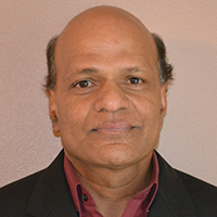
Ashok Kabadi
Managing Director
AK Technology (AKT) Leadership


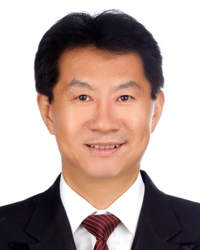
Yoinjun Shi
Yoinjun Shi
CTO
Twinsolution Technology Shanghai

In this tutorial, we will go over the socket contact element fundamentals, types of socket contact elements, contact element materials, and printed circuit board (PCB) & hardware requirements. We will also cover electrical, and system design and test requirements. We will provide you with different options for selecting interconnect sockets depending on your requirements like signal integrity, cycle life, cost, etc.

At the end of the course, you will have a clear understanding of the types of sockets available in the industry, how to select the best one for your needs, and how to successfully develop and implement the same.

Target audience includes: PCB designers, mechanical engineers, hardware engineers, hardware engineering managers, and materials engineers.

Objectives

  • Understand what the interconnect socket is and its benefits
  • Understand the contact elements and resistances
  • Understand different types of interconnect sockets available in the industry and their applications
  • Provide overview of different PCB plating available in the industry and their applications
  • Understand mechanical system design methodologies with special emphasis on tolerances, PCB Keep-Out-Zones (KOZs) and retention design
  • Provide overview of electrical signal integrity measurements
  • Understand test and validation requirements for interconnect technologies
  • Understand the entire end-to-end process flow, right from gathering the requirements to successful implementation

Language: Materials in English. Oral presentation in English and Mandarin.

Fee: 990 RMB / $145 USD - includes Tutorial Guide (printed & electronic copy), buffet lunch, coffee/tea breaks, and certificate of completion.

Note: Attendance at the tutorial will be limited. Please sign-up early to not miss this excellent tutorial!

Ashok Kabadi joined Intel as a Manufacturing Engineer in the Systems Manufacturing Department in 1981. Over his thirty-five year career at Intel, his technological innovations advanced the high-tech industry. His last role was Mechanical Architect and Senior Principal Engineer in the Platform Hardware Group (PHG). Ashok drove the development of multiple advanced platform technologies whichhad significant and measurable impact on improving the cost and time-to-market (TTM) of Intel products as well as external customer products, These technologies included Metallized Particle Interconnect (MPI) sockets, zero keepout (ZKO) sockets, and coax via technology. Ashok was also the key driver for building the Technical Leadership Program in Guadalajara, Mexico (GDC), as well as personally mentoring and growing the pipeline of technical talent in GDC.

He has a deep passion for innovation in the areas of socket interconnect, thermal design, and printed circuit boards. In addition to 16 patents, he has delivered multiple publications, presentations and talks at conferences within the US and internationally. Ashok is now Managing Director of AK Technology (AKT) Leadership providing consulting services and the BiTS Workshop Technical Program Co-chair.

Yoinjun Shi is currently CTO of Twinsolution Technology Shanghai Inc., He has Bachelor Degree of electronic engineering from Suzhou University and MBA from Victoria University Switzerland. Yoinjun has over 15 years’ experience in the semiconductor industry. Now Yoinjun’s major focus is on developing high quality metal contactors. He is a member of the BiTS China Technical Program Committee.

> alt="Link to Session two Presentation three">
BiTS China 2017
Thursday September 7, 2017
8:00 - 9:00
Registration
Please arrive early to check-in and pickup your conference badge and materials prior to the program start.
9:00 - 9:15
Opening Remarks
Welcoming remarks from
Ira Feldman, BiTS Workshop General Chair, and
Steven Zheng, BiTS China Chair
> alt="Link to Opening Remarks">
9:15 - 10:00
Keynote Address
Tingyu Lin
Tingyu Lin
Technical Director
National Centre for Advanced Packaging (NCAP), China
"Fan Out Technology Overview"
"针距扩展(fan out)技术综述"
Tingyu Lin
National Centre for Advanced Packaging (NCAP), China

This presentation provides an overview of the challenges, developments, and solutions of fan out packaging technology including key aspects of patents, technology, supply chain and global players, and market development. The National Centre of Advanced Packaging, China (NCAP China) is also introduced in terms of current work on wafer/panel level fan out packaging. Fan out technology has continued to be developed for the consumer market after the initial TSMC INFO introduction in iPhone 7 (A10 processor) in 2016. As a result, many other types of fan out packaging will be found in the market after 2017. This fan out technology will sharply impact the market as both wafer level and panel level fan out technologies are implemented for high-volume consumer products.

在这次会议中,扇出技术综述的演讲全面介绍了近些年扇出技术的重要方面,如专利,技术种类,供应链发展及全球市场发展的情况。 同时,华进半导体及国内封装厂在扇出技术研发方面也得到了全面的介绍和展示,扇出技术的产业化在2016年后, 特别是台积电为苹果iPhone7 生产出A10 处理器后,其技术特点是INFO 的扇出技术在手机中得到了广泛应用。今后几年随着晶圆级和扳机扇出技术的发展,这项技术对市场的影响会更积极地展现出来。

> alt="Link to Keynote">
Biography (English)

Tingyu Lin

Dr. Tingyu Lin has more than twenty years of experience in design, process, assembly, reliability and equipment development in electronics packaging, semiconductor, consumer electronics, PCBA, thermal and aerospace industry.  He received a B.E. degree in thermal engineering from Tsing Hua University and a M.E degree in aerospace engineering from the Ministry of Aerospace in 1990 in China and a Ph.D in microelectronics from National University of Singapore (NUS) in 1997. He is a Motorola (Google) certified Six Sigma Black Belt in 2012. From 2013 to present, he has been a technical Director of the National Centre for Advanced Packaging (NCAP), China. He is responsible for strategy planning, organizing consortium, and leading R&D activities on advanced packaging material and equipment for the development and commercialization of fan out, TSV, and 2.5D process solutions.  From 2012-2013 he was a program director of the Institute of Microelectronics, Singapore (IME), and responsible for 2.5D, fan-out, and WLP development. From 1997-2012 he worked as a senior manager in Philips, Lucent Technologies (previously AT&T Bell Lab) and Motorola Electronics. where he was responsible for consumer electronics design, process and product development, and advanced manufacturing in advanced IC packaging in flip chip module and SiP, and supply chain management and mobile product quality and reliability improvement.  He has been engaged in more than 100 product design & process development in mobile module, IC component, and consumer electronics, etc.  Dr. Lin had published 150 papers and filed more than 10 patents. In addition to receiving many excellent paper awards and providing keynote talks at several conferences, he drove and passed two international ASTM sputtering material standards(F3166 & F3192)for TSV development. He received several Motorola Innovation awards in 2008。

Biography (Chinese)

林挺宇

  • 中国清华大学(BS);新加坡国立大学 (Ph.D); 阿德莱德大学(MBA)
  • 2014年国家“千人计划”入选者
  • 获得摩托罗拉认证的6Sigma质量黑带,发表论文百余篇,国际专利数十项
  • 先后任职于飞利浦、朗讯、摩托罗拉、新加坡微电子所,目前任职于华进半导体封装先导技术研发中心有限公司,担任技术总监(扇出型封装工艺、材料、可靠性与失效分析方向)、战略研究与产业化部长
10:00 - 10:30
Market Report
An overview of the test consumables market:
"Opportunities and Challenges of the Chinese Test and Burn-in Sockets Market"
"半导体芯片性能和寿命测试插座的中国市场"
Lin Fu
VLSI Research Europe
John West
VLSI Research Europe
> alt="Link to Keynote">
Abstract and Biography (English)

China has become a key market for test and burn-in sockets and has created opportunities in both directions: foreign suppliers wanting to enter the country, and emerging domestic suppliers looking to export to other regions. This presentation analyses the supply and demand status of test and burn-in sockets for the Chinese market and outlines the challenges facing foreign suppliers as well as the prospects for Chinese companies as a result of this geographical shift.

Lin Fu received the Bachelor Degree in Electrical and Electronic Engineering with first class honours from Edinburgh University in 2013. Then, she started her postgraduate study in Cambridge University. In the meantime, she published more than ten papers as the first author or co-author in the IEEE Transactions on Applied Superconductivity, Superconductor Science and Technology, Applied Physics Letters and so on. In 2017, she received the doctoral degree in Engineering from Cambridge University and started to work in VLSI Research Europe. At present, she focuses on the marketing research and analysis related to semiconductor test consumables, including probe cards, test and burn-in sockets and device interface boards.

Abstract and Biography (Chinese)

中国市场逐渐在半导体测试领域发挥关键作用,并且创造了许多双向的机遇:外国供应商希望进入中国市场,同时本土新兴的供应商也希望拓展海外业务。

在此次展示中,我们将分析中国市场 test 和 burn-in sockets的供求现状,概述国外及本土供应商所面临的诸多挑战。

付琳于2013年毕业于爱丁堡大学,并获得电气与电子工程一等荣誉学士学位。同年,在剑桥大学继续研究生学习。期间,她作为第一作者或合作者在国际期刊及会议上发表论文十余篇。2017年,付琳取得剑桥大学工学博士学位并开始在VLSI Research Europe工作。目前,她致力于半导体测试领域的市场研究与分析,包括探针卡,测试插座及设备接口板等。

10:30 - 11:00
Break

Enjoy time to meet with the presenters and network while refreshments are served.

11:00 - 12:30
Session 1
RF & High Speed Test
Radio frequency and high speed test challenges
Regional and global experts will share their expertise and solutions to the challenges of high frequency / speed and radio frequency (RF) test.

Technical presentations in English or Mandarin. Slides in English with bilingual question & answer period.

"High Speed Testing"
"高频测试"
Jackie Luo
Shanghai Zenfocus Semi-Tech Co., Ltd
> alt="Link to Session one Presentation one">
Abstract and Biography (English)

High Speed Testing is moving from some independent modules to an integrated complex system. In order to make sure that the final system can meet testing requirement, we need to do complete correlation between simulation and verification of each segment, then we can do fully correlation between the simulation and verification of the whole system.

This presentation covered four topics, firstly, it introduced some typical 100G high-speed interface such as SFP+, QSFP+, miniSAS, zSFP+, zQSFP+, CXP, CFP, CFP2, CFP4 coming along with the age of BIG DATA. Secondly, it covers the testing of a 100G high-speed interface based on IEEE802.3bm(CAUI-4)and IEEE802.3bj. Thirdly, it describes how to design a workable 100G testing fixture, starting with material verification, stackup design, trace impedance tuning and insertion loss correlation, then it summarized some methods to optimize vias and connector mating to get requested impedance control, insertion loss, cross talk, common to differential mode conversion, etc. Fourthly, this presentation used keysight PXI Modular network analyzer to do the fixture verification based on PLTS, to get the comparison result with IEEE802.3bj Spec.

Jackie Luo is founder and President of Zenfocus Corporation who is subsidiary of Shenzhen Fastprint Circuit Tech Co., Ltd., starting from August 2015, Prior to founding Zenfocus, Jackie worked as Asia-Pacific Manager of Pactron, in charge of overall business development, engineering and supporting for three years.

Before doing ATE board business, Jackie worked as senior application engineer in Verigy (now Advantest) for 5 years and worked as staff test engineer in Spreadtrum for one year. Jackie Luo received his B.A from Nanjing University, a Master Degree of information and communication engineering from Zhejiang university.

Abstract and Biography (Chinese)

伴随着测试技术的飞速发展,高速测试从一些相对独立的模块逐渐整合成为复杂的系统级测试。为了满足终端系统能够达到测试要求,我们需要逐段进行仿真和验证,从而最终能够满足整个系统的仿真与验证需求。

本篇论文包括四个主题:
首先,介绍一些伴随大数据时代而产生典型的100G高速信号,例如SFP+,QSFP+,miniSAS,zSFP+, zQSFP+, CXP, CFP, CFP2, CFP4等;
其次,它涵盖了基于IEEE802.3bm(CAUI-4)和IEEE802.3bj的100 g高速接口的测试;
再次,我们从选材,叠层,阻抗优化,插损等方面来描述如何审计一个可行性的100G高速信号的测试夹具,然后总结了一些优化过孔,连接器匹配等方法以满足阻抗控制,插损,串扰,和差模转换的需求;
最后,我们用基于PLTS的keysight PXI的网分仪量测的结果与IEEE802.3bj的Spec进行对比。

Jackie Luo
是上海泽丰半导体科技有限公司的创始人和总经理,上海泽丰半导体科技有限公司是2015年8 月成立的深圳市兴森快捷电路科技股份有限公司旗下的子公司。在此之前,他曾担任三年的Pactron亚太区的总经理, 负责Pactron在亚太地区的业务发展,和工程及技术支持。 在专注于ATE的测试板业务前,Jackie曾在惠瑞捷(现爱德万)任职高级应用工程师五年,后又在展讯通信任职测试工程师一年。 Jackie Luo在南京大学取得学士学位,后于浙江大学信息与通信工程取得硕士学位。
"Flat Probe Technology for RF Test"
"高频测试用扁平型探针"
Dongmei Han
Xcerra
Jason Mroczkowski
Xcerra
Nadia Steckler
Xcerra
> alt="Link to Session one Presentation two">
Abstract and Biography (English)

Today the semiconductor test market is very competitive. This is especially true in the consumable contactor market.

Low operating costs and low average selling prices create low barriers to entry. Micro-organizations plant themselves next to their sole customer and provide fast turn times at competitive prices and onsite support. Although this is acceptable for some it is a risky business model. Furthermore the depth of knowledge of the product and therefore the value add from these micro-organizations is limited.

Outsourcing components can diminish the value add of the end product and lead to finger pointing and delivery delays. These factors push organization toward more stable and established vendors that can not only provide fast turn times and good support but they can focus on R&D and new product development. The ability of these organizations to fund R&D has resulted in revolutionary “flat probe” technologies that combine both electrical and mechanical performance at a significantly lower cost point than traditional radial spring probe technologies.

Larger spring diameters allow more force with less spring length allowing shorter and narrower probes than possible with radial technology. Furthermore the external plunger surfaces allow superior plating than in the internal surfaces of a barrel. Hard base materials offer longer life with lower contact resistance. Finally, with proper attention to the “guts” of the probe design, flat probe technologies can be used for high frequency semiconductor test applications. This presentation will introduce various flat probe technologies and compare and contrast their designs against other flat probe technologies as well as against radial probe technologies.

DongMei Han is a Signal Integrity Project Manager/Engineer with Xcerra Corporation. She is currently working on over the air mmWave test sockets with a bandwidth of over 100 GHz. DongMei holds a Master of Engineering degree for the University of Illinois. DongMei started her career with Motorola in the Cellular Subscriber Division where she worked as an Analyzer Engineer and Team Leader. DongMei later joined the Tyco Safety Products group in Canada where her work included system and board level RF design and test, including transmitters, receivers used for ISM band applications. This work included RF and analog circuitry including filters, amplifiers, switches, LNAs, PCB antennas, PLLs, VCOs, AGC, and matching network. Before joining Xcerra, DongMei was involved with RF antenna theory, electromagnetic modeling, and energy harvesting devices, along with wireless sensors, and wireless systems architectures.

Abstract and Biography (Chinese)

今天的半导体市场竞争非常激烈,特别是在消费电子接触领域。

较低的运营成本和较低的平均销售价格使得这个市场比较容易进入。靠单一客户的微小工厂可以提供极具竞争力的价格和在线技术支持。虽然大部分时候这个是被接受的,但是这是一个非常危险的商业模式。此外小型公司无论是对产品的知识程度和深度还是对客户领域的了解和增值服务是非常有限的。

组件的外包大大降低了产品的附加值并最终导致相互指责和交期延误。

诸多因数促成客户向着更稳定更长久的供应商,那些能够提供不仅快速的交期,及时的技术支持,而且能够专注在新产品开发上面。这些在研发上面投入大量资金的供应商已经开发出了革命性的片状探针技术,其不仅能够提供优越的电气和机械性能,而且价格还比传统螺旋弹簧探针的产品低。

更大的弹簧直径允许更多的力量与较少的弹簧长度允许更短和更窄的探头比径成为可能。此外,顶针外表面表面比套筒的内表面上电镀要容易。较硬的基材具有更低的接触电阻,寿命更长。最后,适当注意探头设计,片状探针技术可用于高频半导体测试应用。本文将就片状探针技术进行探讨同时比较不同种片状探针技术的差异,以及片状探针和弹簧探针技术的区别。

DongMei Han
韩冬梅是Xcerra公司的信号完整项目经理/工程师。她目前正在研究超宽带宽度为100GHz的mmWave测试插座。 冬梅拥有伊利诺伊大学工程学硕士学位。冬梅在摩托罗拉开始了她的职业生涯,在蜂窝用户部门担任分析工程师和团队负责人。 冬梅后来加入了加拿大的Tyco安全产品集团,她的工作包括系统和板级RF设计和测试,包括用于ISM频段应用的发射机,接收机。 这项工作包括RF和模拟电路,包括滤波器,放大器,开关,LNA,PCB天线,PLL,VCO,AGC和匹配网络。在加入Xcerra之前, 冬梅还参与了射频天线理论,电磁建模和能量采集设备,无线传感器和无线系统架构

"Coplanar Waveguide On Wafer Calibration Technology for Enabling High Volume Microwave On-Wafer Test"
"共面波导在片校准技术使微波集成电路在片量测成为可能"
Yuzhe Yin
China Electronics Standardization Institute
> alt="Link to Session one Presentation three">
Abstract and Biography (English)

Microwave power amplifiers such as GaAs/GaN can operate at 40 GHz and beyond. Those III-V PAs were previously measured by separated instruments such as network analyzer/signal generator and power meters, since automated test equipment (ATE) could only handle 6 GHz. And semi-automatic probe-stations were used to extended the test plane to wafer. However, this approach is of low efficiency. Even worse, the sophisticated 5G modulated signal test and multiple wireless protocol combination test will greatly increase the whole system complexity creating a nightmare. ATEs such as the Advantest V93000 provides the intrinsic advantage of high levels of integration enabling complex 5G modulated signal wafer level test. However, currently the 93K can only handle power or insertion loss related calibration due to the scalar calibration process. The S parameters of the load board is still unknown, which accounts from the coaxial interface to probe needle end. In some critical applications such as device modeling, the calibration plane should expend even further right up to the edge of the pHEMT or HBT. This presentation details a GaAs calibration standard chip that was developed. This standard chip provides SOLT and TRL calibration cells at least covering 40 GHz. VSWR and Insertion loss verification cells were also included. In addition, a novel TRL on wafer calibration algorithm is introduced that combined with the standard chip enables high volume production microwave testing on-wafer.

Yuzhe Yin received his bachelor and master’s degrees from Physics Dept. and PhD from Electronic Engineering Dept. Of Tsinghua Univ. He is now working in China Electronics Standardization Institute(CESI) as the team leader of solid state IC and optics. His research focuses on solid state IC related standards, verification and test/metrology technology. He has developed CESI 8190 GaAs coplanar waveguide standard chip and CESICalkit calibration software. Now he is working on GaN and silicon RF IC test and metrology technology such as RF-MEMS and RF-SOI

Abstract and Biography (Chinese)

类似于GaAs/GaN的微波功放已经可以工作到40GHz以上。这些三五族化合物半导体功放以前是采用分立仪表测试的, 包括矢量网络分析仪、信号发生器和功率计。自动测试系统ATE还只能覆盖到大约6GHz范围。 半自动探针台可以对分立仪表系统进行扩展以完成在片量测。但这种方式既不经济也难以适应5G复杂调制信号的量测需求,测试系统会异常臃肿。 类似于Advantest V93000的ATE自动测试系统具有高集成度、适合复杂调制信号测试等先天优势。但是目前93K还只能进行类似于功率、插入损耗等标量校准。 从同轴接口到探针针尖的载板S参数还未能校准。在某些严苛的测试要求中,校准参考面甚至需要从探针针尖迁移到管芯, 精确提取出pHEMT或HBT管芯的性能参数。本文详细介绍了GaAs共面波导标准样片的设计,它可以提供SOLT和TRL的校准, 覆盖到40GHz以上。驻波比和插入损耗检验模块也在其中。一种适用于该样片的TRL在片校准算法和自动校准软件也被提出, 与标准样片可以共同完成ATE在片量测系统的矢量S参数校准。

Yuzhe Yin
殷玉喆,博士。清华大学物理系获得固体物理专业学士、硕士;清华大学电子工程系获得物理电子学博士。 殷玉喆目前是中国电子技术标准化研究院固态器件与光学音视频组组长,常年开展固态微波功率器件相关标准制定、鉴定检验、计量测试技术方面研究。 研制了CESI8190型GaAs共面波导校准检验片及CESICalkit校准软件,目前正在开展GaN及硅基RF-MEMS、RF- SOI相关计量测试技术研究。

12:30 - 14:00
Lunch &
BiTS EXPO
BiTS EXPO
opens at 13:00
Enjoy the delicious hot buffet lunch and networking time. Then take the time to explore the BiTS EXPO. There will be many great exhibits to explore what is Now & Next in the test and burn-in of semiconductors. You will be certain to see something new or meet someone new.

As attendees to BiTS know, there is always excellent food, drinks, and time for attendees to network with exhibitors!

BiTS EXPO will open at 13:00 and will remain open throughout the afternoon until 18:00

14:00 - 15:00
Session 1 Continued
RF & High Speed Test
Radio frequency and high speed test challenges
Regional and global experts will share their expertise and solutions to the challenges of high frequency / speed and radio frequency (RF) test.

Technical presentations in English or Mandarin. Slides in English with bilingual question & answer period.

"DUT ATE Test Fixture S-Parameters Estimation using 1x-Reflect Methodology"
"采用 1x-反射法解析芯片自动测试夹具的 S-参数"
Jose Moreira
Advantest
Ching-Chao Huang
AtaiTec Corporation
Derek Lee
Nvidia
> alt="Link to Session one Presentation four">
Abstract and Biography (English)


ATE Test fixture loss is a critical factor for high-speed digital and high-frequency RF applications. Measuring the test fixture loss is not a trivial task especially due to the challenges of probing a DUT socket. Most test engineer’s lack of experience, the time and the equipment to perform this kind of measurement. But understanding the test fixture loss is critical for verifying the correct design and manufacturing of the ATE test fixture, de-embedding the measurement results and set the correct equalization setting on the ATE digital pin electronics.

In this presentation we will describe a methodology to obtain the ATE test fixture s-parameters using a single return loss measurement with no DUT in the DUT socket (i.e. 1x-reflect into open). We will describe the methodology, its advantages and drawbacks and present some result examples using real ATE test fixture examples. This 1x-reflect methodology is not new in the test and measurement community and it is supported by several software vendors but it is not widely known by the ATE testing community. Also test engineers have difficulty in understanding how to use a de-embedding methodology in their ATE application development process. In this presentation we plan to show how it can be used by showing real examples.

We will show that this kind of measurement can be done already after the manufacturing of the ATE test fixture not requiring an expensive ATE system requiring only a minimal set of equipment.

Jose Moreira received a Licenciatura and M.S. degrees in Electrical and Computer engineering from the Instituto Superior Tecnico of the University of Lisbon. He was with Agilent Technologies and its spin-off Verigy since 2001 which was later acquired by Advantest. He is currently a senior R&D staff engineer at Advantest Germany. His research interests are signal and power integrity, multigigabit interfaces characterization and test fixture design and measurement. He is co-author of the book “An Engineer’s guide to Automated testing of High-Speed Interfaces”.

Abstract and Biography (Chinese)

高速及射频类半导体芯片测试中, 测试夹具的信号损耗是一关键参数。因芯片测试座的高频性能测量装置非常复杂, 测量其信号损耗不是件容易的任务, 多数测试工程师缺乏经验,时间和装备去做此测试, 但是充分理解插座的信号损耗会有助于芯片测试座的设计和制造,解析芯片测试结果及建立正确的电子方程。

本文将介绍一个方法去测量自动测试座的S-参数,此方法是单个信号测量的单侧固体座(无芯片在测试座中)。将介绍其方法和其优势及缺点。 该1X-反射技术不是新方法,已广泛应用于其它测试行业。并有多个软件供应商。但是没有用于芯片自动测试业, 同时工程师难于理解和掌握数据的解析方法, 本文将举例并说明这类方法。

本方法将显示这类的测量方法不需要大型且昂贵的自动测试机,仅需要小型而且简单的测量装置。

Jose Moreira 毕业于里斯本技术大学电气和计算机工程系,获得理科硕士学位. 他目前担任Advantest德国公司的高级工程师。从2001年, 他曾在Agilent Technologies的测试部Verigy工作, 后该测试部被Advantest收购。 他的研究领域包括信号和功率完整性,高频(千兆级)连接界面特性和测试制具, 他还是Artech House 出版的《测试高速接口自动化测试设 备【Testing High‐Speed Interfaces with Automated Test Equipment】》一书的联合署名作者。

"Contactor Arcing Fundamentals"
"触点拉弧基础"
Abstract and Biography (English)

As early as 1801 arcing was described by Sir Humphry Davy who observed it between two carbon electrodes. Due to natural convection, the hot gas moves upward causing the arc of the carbon electrode to bend upwards and form an arch. Hence people call this phenomenon an "Electric Arc" (the arc of electricity).

As digital signal speed has increased significantly in the past a few decades,the switching time of electronic circuits has been greatly reduced. When the switch closing time becomes too short, it prevents the electrical energy stored in the circuit from being discharged before an electrical contactor or probe is removed. Thereby this potential voltage difference between the contactors pair has the risk of causing the arcing. Once arcing occurs it will shorten the life span of the contactors and it is observed that some contactors turn black after a given number of insertions.

This presentation will examine different material versus contactors pair spacing versus arcing voltage. And based on the experimental data collected we built a simulation model based upon Maxwell’s equations. With this simulation model we can study further about the inductance of the probe and tip shape design impact to the arcing risk

Yoinjun Shi is currently CTO of Twinsolution Technology Shanghai Inc., He has Bachelor Degree of electronic engineering from Suzhou University and MBA from Victoria University Switzerland. Yoinjun has over 15 years’ experience in the semiconductor industry. Now Yoinjun’s major focus is on developing high quality metal contactors. He is a member of the BiTS China Technical Program Committee.

Abstract and Biography (Chinese)

早在1801年,H.Davy先生就发现了电弧。最早被观察的电弧是在两个碳电极之间点燃的,由于自然对流的作用,热气体向上运动, 使碳电极的电弧向上弯曲而形成为拱形,因此便被命名为Electric Arc(电的拱形物),这就是电弧名称的由来。在过去的几个世纪以来数字信号的速度原来越快,电子开关开关的时间越来越短, 过快的关断时间使得储存在探针上的电能无法释放,从而在探针针头和芯片引脚之间产生压差并导致拉弧的风险当探针和芯片分离的时候, 一旦发生拉弧探针的寿命将会受到影响或者比较容易观察到的一段接触以后针头变黑。 本文通过对不同材料的电极的实验数据得到相关的拉弧电压和触点对之间的距离。并根据实验数据建立相应的Maxwell仿真模型。 从由仿真模型进一步探讨探针感抗和针尖的设计对拉弧风险的影响。

Yoinjun Shi
施 元军目前是上 海韬盛电子科技股份有限公司的研发经理。他在半导体测试产业有超过15年 的经验,并致力于测试连接器对信号和电源完整性影响研究多年, 他还多次提交并获得专利。其中以高 隔离度的测试插座的研发最具代表性。现在他主要专注于开发低接触电阻和长寿命的金属接触探针。

15:00 - 15:30
BiTS EXPO
& Break
BiTS EXPO Continues
Enjoy additional time to meet with the presenters, network, and explore the BiTS EXPO further. There will be many great exhibits to explore what is Now & Next in the test and burn-in of semiconductors.

Afternoon refreshments will be served.

15:30 - 17:30
Session 2
SiP Test & Contact Technology
Latest presentations on challenges of SiP test and contact technology
Hear up-to-date local presentations from across Asia describing semiconductor test and burn-in challenges. These regional and global experts will share their expertise and solutions to these challenges.

Technical presentations in Chinese or English as noted. Slides in English with bilingual question & answer period.

"The challenge of testing and burn-in for System in Package"
"系统级封装芯片的测试及老化实验的挑战"
alt="Ribbon for best Paper">
Leo Wang
ISE Labs, member of ASE Group
> alt="Link to Session two Presentation one">
Abstract and Biography (English)

System-in-Package (SIP) packaging has greatly increased in popularity due to mobile device size requirements. However for system level package it brings many challenges to mass production testing and High Temperature Operating Life (HTOL) testing. This presentation will discuss SIP’s testing throughput and efficiency and the future needs to support SIP level HTOL testing requested.

Leo Wang is currently the Director of Engineering in ISE Labs, a member of ASE Group. With over 12 years of experience in test engineering, he was in charge of setting up ISE Labs Shanghai in 2014 to provide leading engineering environment for ATE testing and qualification service to local companies. Leo received his bachelor's degree in Electronic Engineering from Zhejiang University, China.

Abstract and Biography (Chinese)

由于车用芯片的特点,SIP (System-in-Package) 封装芯片快速增长。但是此类封装芯片给大批量特性和高温寿命(High Temperature Operating Life) 测试带来众多挑战。本文将讨论这些挑战并提出解决方案和将来的需要。

王钧锋先生现任ISE Labs总监。ISE Labs是日月光集团提供測試服務的子公司。 王先生拥有超过12年的测试经验,并于2014年设立ISE Labs上海实验室,提供中国內地公司完善与先进的ATE测试与质量测试认证等服务。 王钧锋毕业于浙江大学电子工程学系。

"Socket Material Characterization & Selection"
"芯片测试插座材料特性和应用"
Jinrong "Cleveland" Chen
Smiths Interconnect
Jiachun "Frank" Zhou
Smiths Interconnect
> alt="Link to Session two Presentation two">
Abstract and Biography (English)

Material choice is recognized as a key element in Semiconductor package testing and remains a challenge for both end-users and test socket design engineers. Factors considered in the selection process include:

  • Variety of material options and their various applications
  • Difference between material specifications and its performance in actual applications: comparing results of published specifications is not sufficient.
  • Balancing end-user expectations with socket designer recommendations: customers often specify one material when better options are available.

Smiths Interconnect has performed extensive studies focused on characterizing several materials in order to optimize material selection for socket design. As we know, the traditional test socket structure consists of a two-piece body, designed to retain spring probes, with an alignment plate or floating base integrated for package alignment in manual or auto test.

Key concerns and recommended material solutions will be discussed in this paper:

  1. Material strength: The socket must sustain the spring probe’s preload force especially for high pin count or short test length applications. Flexural strength and modulus are major considerations. A compound socket structure, with a metal frame to improve the housing component’s strength, is also a solution. Impact strength may also be a concern for socket designs without a docking plate.
  2. Dimensional stability: Water absorption and CLTE are two major factors. Dimensional stability is critically important especially in fine pitch and multi-site test sockets, such as our Volta WLCSP socket. Extensive experiments have established correlations between dimensional variation and water absorption. A new Peek material, developed by Smiths, offers improved strength with greater dimensional stability.
  3. Wear resistance: Identifying the component most likely to encounter wear is key. In a traditional socket design, this is typically the alignment plate or floating base. However, with a socket design using stamped contacts, such as Smiths Interconnect’s Celsius Socket, wear on the slot feature wear may require attention as well. The comparison of wear resistance testing provides information critical in material selection.
  4. Thermal properties: Continuous service temperature and heat deflection temperature (HDT). This should be evaluated considering the end user’s test environment and duration.
  5. RF performance: The material’s dielectric constant affects test socket RF performance. There is not a significant variance in the dielectric constants of commonly used socket materials. Because of this, for high speed testing, consideration is given to the use of both special materials, such as IM material, as well as a coaxial socket design structure.
  6. Manufacturing capability, efficiency and cost: Socket machining feasibility varies from material to material. The study uses one machining coupon to compare the machining feasibility of each material, as well as the machining efficiency and tool cost.

In order to verify material selection, this paper will discuss the simulation tool’s FEA (benefits and limits), relevant test data of the evaluated materials and customer experimental data. The materials include Peek, Vespel, MDS100, Ultem, Torlon, Tecapeek, IM. In summary, no "perfect" material exists for use in all socket types. Understanding material characterizations provides the opportunity to select the optimal socket material to meet the application’s requirement.

Cleveland Chen graduated from Nantong institute of technology in 1999, majored in Process and Equipment of Machinery Manufacturing. He has worked in Semiconductor IC testing industry for 12 years and is now the Semi manager of R&D, smiths interconnect Suzhou.

Abstract and Biography (Chinese)

在半导体芯片测试插座设计中,材料选择是关键要素之一,对于设计工程师来说仍是一个挑战。材料选择环节需考虑:

  • 不同材料的比较
  • 材料性能和应用上的差异
  • 用户的期望与设计方案的平衡

史密斯英特康研究了多种材料特性以选择最优化的材料。

本文讨论材料选择的关键参数及优化的测试插座材料。

  1. 材料强度:插座须承受探针的预压力,尤其是高探针数量及短针的插座体。材料挠曲强度及模量是主要参数。采用金属框复合插座结构可增加探针座体强度。对于一些特殊的插座,抗冲击强度也是重要参数。
  2. 尺寸稳定性:吸水性和线性膨胀系数是主要决定因素。其对于小节距及多工位测试插座尤为重要,如WLSSP测试插座。对于材料尺寸变化及吸水性的关系做了广泛的实验后,史密斯开发出一种新型材料,具有更高的强度及尺寸稳定性。
  3. 耐磨性能:传统的插座设计中的导向板或浮动座; 对于冲压成型接触片的插座,如史密斯英特康的Celsius插座中针槽的磨损。抗磨损试验结果比较有助于材料选择。
  4. 热性能:持续工作温度及热变形温度(HDT);需考虑最终用户的测试环境及持续时间。
  5. 高频性能:材料介电常数影响插座的高频表现。常用的插座材料的介电常数没有明显的差异。正因如此,对高速测试,需要考虑应用如IM的特殊材料及同轴结构。
  6. 制造性能,效率和成本

还会采用FEA,材料验证的测试数据及客户的试验数据来确认材料的选择。讨论的材料包括Peek, Vespel, MDS100, Ultem, Tolron, Tecapeek 及IM等。没有“完美的材料”可用于所有的插座。 理解材料的特性为我们选择最优化的材料提供可能

Cleveland Chen
陈金荣,于1999年毕业于南通工学院,机械制造工艺及设备专业。从事半导体芯片测试行业工作12年,现在是史密斯英特康半导体事业部(苏州)的研发部经理。

"Deterministic contact resistance of BGA contact pins"
"BGA 测试探针的接触电阻研究"
Terry Wang
Infineon
Praveen kumar Ramamoorthy
Infineon
Yusman Sugianto
Infineon
> alt="Link to Session two Presentation three">
Abstract and Biography (English)

It’s a well-known fact that the price of semiconductor devices fall from 5% – 20% every year. This persisting trend since a decade has led to an increased pressure in reducing the testing cost of the devices. A significant portion of the spending is for consumables such as sockets and contact pins. Among these, contact pins are replaced more frequently than the socket housing.

In order to understand reasons behind end of life of the contact pins a fundamental study was performed on determining the contact resistance of BGA sockets at lab that run through various intervals at production, as contact resistance is the important factor for defining end of life of the sockets at production. Socket analyser was used for measuring the force and resistance of all the pogo pins in the socket and three repeated measurements were performed to check repeatability of the data acquired. Stroke was fixed at the value similar to that of production and a socket with fresh pins was taken as reference.

Measurement results for the end of life pin at 90k revealed 15 – 20% reduction in pin force with 6x increase in in contact resistance. The contact pins were further examined through high resolution scope (1000x capability) to understand the wear and tear mechanism at various touchdowns. It was also observed that there was 30 to 50um reduction in pin height in comparison to fresh pins. These findings led to the conclusion that fatigue of the contact pin led to reduction in pin force and thus increase in contact resistance which was further complemented by the wear and tear of the pin tip. So, to achieve higher lifespan of the contact pin material hardness has to be increased with further refinement in the pin tip geometry.

Thus, the lab study was crucial in identifying the root cause behind the failure and to address it accordingly

Xiaojun (Terry) Wang graduated from Beijing University of Aeronautics and Astronautics in 1991, and received Master’s degree in Mechatronics from National University of Singapore in 1999. He has 20 years of semiconductor testing experience. In Infineon, he works on the both FrontEnd and BackEnd test, in charge of probing capability tooling up and BE test contact technologies. His expertise areas are probing technologies, electrical contact solutions and test interface hardware.

Abstract and Biography (Chinese)

众所周知,半导体器件的价格每年下降5%至20%。几十年以来的这种持续趋势, 导致设备测试成本的降价压力越来越大。 生产性支出的很大一部分是消耗品,如测试插座和测试针,特别是测试针需要很频繁地更换。

为了准确地理解测试针寿命的机理,我们在实验室进行了一项基本研究,研究测试插座在实际生产过程中的测针接触电阻的变化。接触电阻是测试针在实际生产中决定寿命长短的重要因素。 研究中使用了 测试插座分析仪, 测量了测试插座中弹簧测针的接触压力和电阻,数据重复测量三次以保证其可重复性。测试针施加的压缩度与实际生产一致。研究中,用了全新的测试插座和测试针作为参考数据值。

测试针寿命的测量结果在九万次时显示出15〜20%的接触压力降低,接触电阻增加了6倍。在高分辨率(1000倍)显微镜下, 进一步检查不同使用程度时的磨损机制。还观察到, 与新针相比,针头还降低了30至50微米。从这些发现可以作出这样的结论:测试针头的疲劳磨损, 导致了接触压力减小,从而接触电阻相应增加。因此,为了实现更高的测针寿命,必须提高针头的耐磨度和优化针头的几何形状。

实验室研究对于确定磨损机理和相应地解决问题是很关键有效的。

Xiaojun (Terry) Wang

王晓军于1991年毕业于北京航空航天大学, 并于1999年获得新加坡国立大和机电一体化硕士学位。他拥有20年半导体测试工厂实际生产和研发经验。
在英飞凌,他负责晶圆测试技术和成品测试电接触解决方案。他的专长领域是晶圆探测技术,成品测试技术和测试硬件开发等。

"New universal multi-beam Kelvin contactor concept for turret applications"
"新型多功能开尔文接触探针设计"
Mathias Westenhuber
Cohu
Johann Pötzinger
Cohu
> alt="Link to Session two Presentation four">
Abstract and Biography (English)

Cost of test requirements for todays and future contactors require solutions, which increase lifespan as well as yield performance within a test cell. Furthermore, resistance stability, signal integrity, as well as current capability provide additional challenges, which need to be considered for any new high performance solution. Especially at applications which are used on to a turret test handler system, the throughput typically is extremely high, and contactors which can overcome electrical requirements need to provide an exceptional good lifespan and stability to minimize any intervention during high volume production. Another mechanical challenge come from smaller package types, which makes it more and more difficult to place one or more (Kelvin applications) contact springs on to one device pad/lead.

Semiconductor customers demanding new contactor solutions, which can accommodate the need for more stable and long lasting contactors solutions. The increasing degree of automation in the final test environment drives the trend towards less human effort to setup, maintain and service test contactors. Repeatable and stable contact resistance behavior in combination with a maximum lifespan are the right answers to this requirement. On the other hand, the trend in the analog/power market drives the need for contactors, which can go beyond traditional performance levels – combinations of low inductance with high current and or Kelvin capability are just some examples of this trend.

The presentation shows a new contact element concept which is based on completely new architecture (multi-beam) as well as a manufacturing process. The concept will push the envelope a bid further to get rid of some of the current limitations socket manufacturers see today. The paper will show an alternative way to generate contact elements with a very small form-factor, which is important to overcome lifespan and stability needs in combination with a new Kelvin architecture, which provides a self-cleaning contact scrub in order to enable low and repeatable contact resistance performance. The new and innovative architecture also allows driving standardization toward generic contactor concepts in the field of turret handling systems. Real high volume production data will be shown and compared to traditional solutions to show the potential of this new Kelvin contactor concept.

Mathias Westenhuberis the Business Development Manager for COHU ITS (Integrated Test Solutions). He coordinates all Sales & Marketing activities and leads the Application Engineering Team. Previously Mathias was the Sales Manager Europe for COHU`s Handler Business.

Prior to that he was the Global Service Manager for RASCO Gravity Feed Handlers and has also held management positions in handler assembly and quality assurance (QA). Mathias earned a “Communication Electrician Engineer“ degree from the Technical College for Electrical Engineering in Munich during his apprenticeship at Deutsche Telekom.

Abstract and Biography (Chinese)

芯片测试市场不断追求新型接触探针,以提高使用寿命,更高的产出,稳定的接触电阻,更高频的信号及承担更高的电流。尤其是在测试机台上的探针塔需要接触探针在大批量芯片测试中保持稳定的性能, 随着芯片尺寸的减小,在单个接触脚上更难于采用 Kelvin(双线)连接方式。另一方面,随analog/power芯片市场的增长,需要更小电感的接触探针。

本文将介绍一种采用新型结构(multi-beam)的接触探针。该探针采用新制造工艺,突破现有探针的局限性,使得探针性能更优。此探针具有如下优点:精细且尺寸小,Kelvin连接,及自清洁,从而保证稳定的低接触电阻。这一新型的结构还可促进探针及测试机上探针塔的标准化。

大批量生产的实际数据与传统探针的性能比较,及该结构的潜质都会在演讲中介绍。

Mathias Westenhuber 是 COHU 公司,ITS(Integrated Test Solution)分公司的市场发展经理。协调销售和市场部的工作,并领导客服工程师部门。曾经担任过COHU的芯片测试装料机 (Handler) 业务的欧洲区销售经理。

Mathias 担任过RASCO芯片自动装料机 (Handler) 的全球销售经理,并担任过多个不同部门的管理职务。Mathias 拥有慕尼黑电子工程技术学院的“通信电子工程师”学位。

17:30 - 18:00
BiTS EXPO
BiTS EXPO Continues

Enjoy additional time to meet with the presenters, network, and explore the BiTS EXPO further. There will be many great exhibits to explore what is Now & Next in the test and burn-in of semiconductors.

Program subject to change without notice.