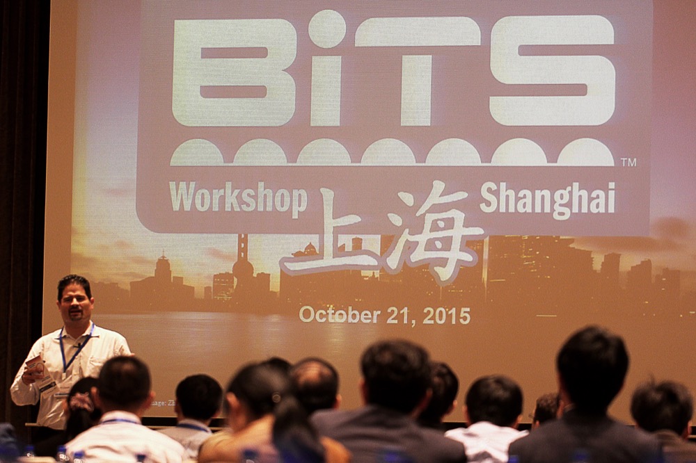
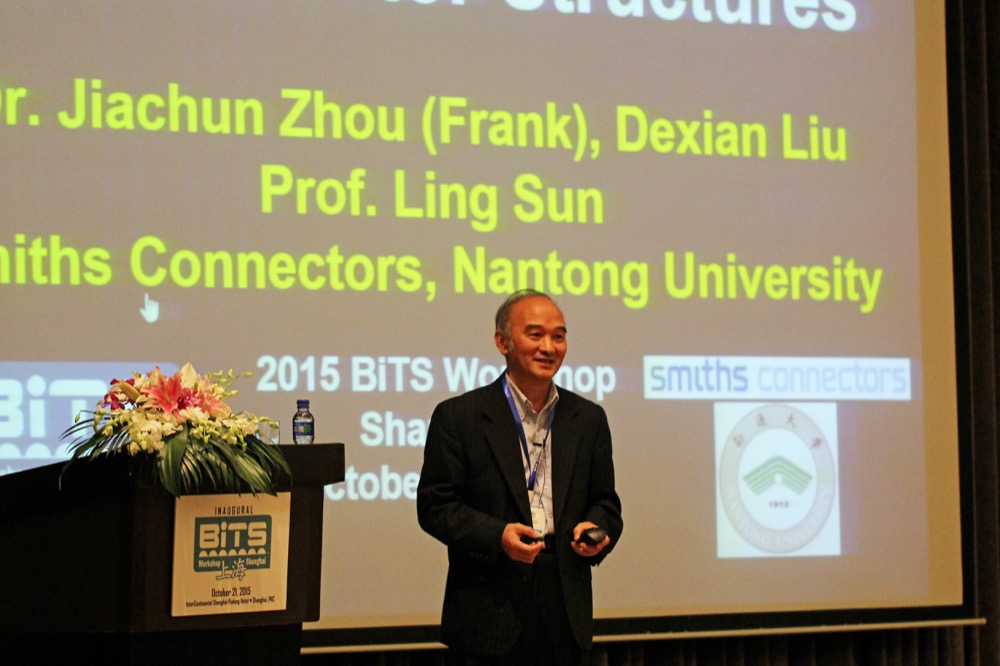
BiTS Shanghai 2015 Archive Program

Join us for the inaugural BiTS event in Asia!

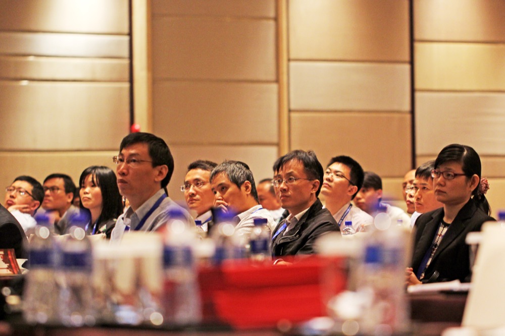
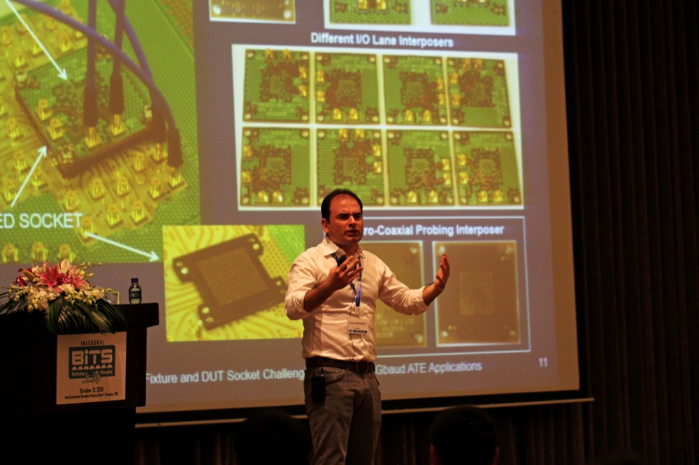
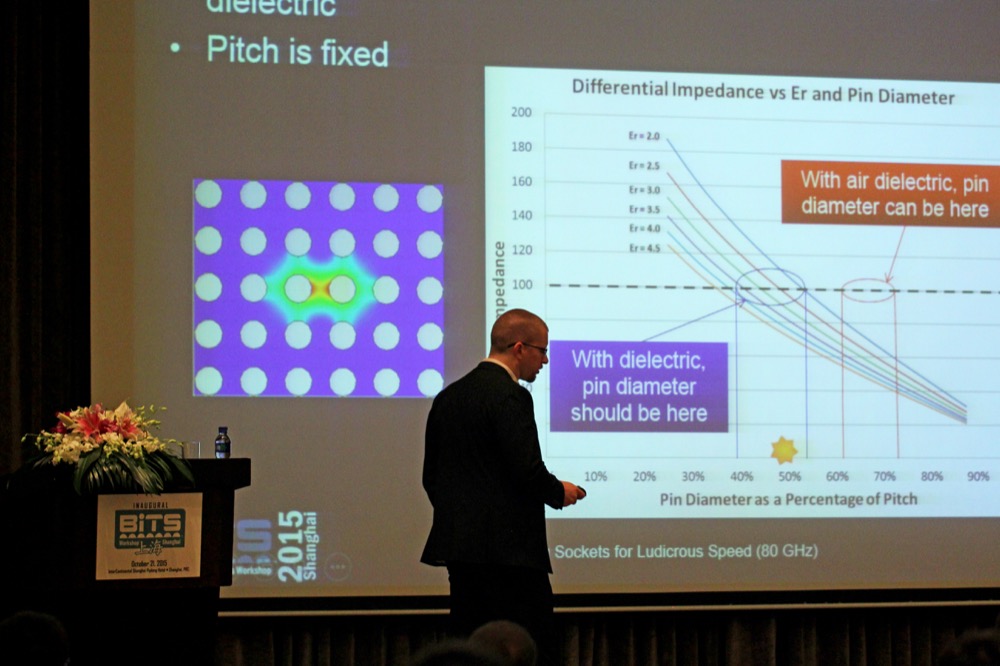
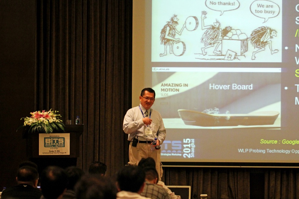
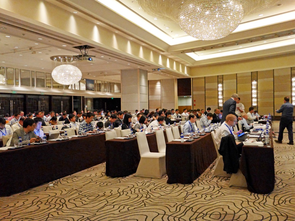
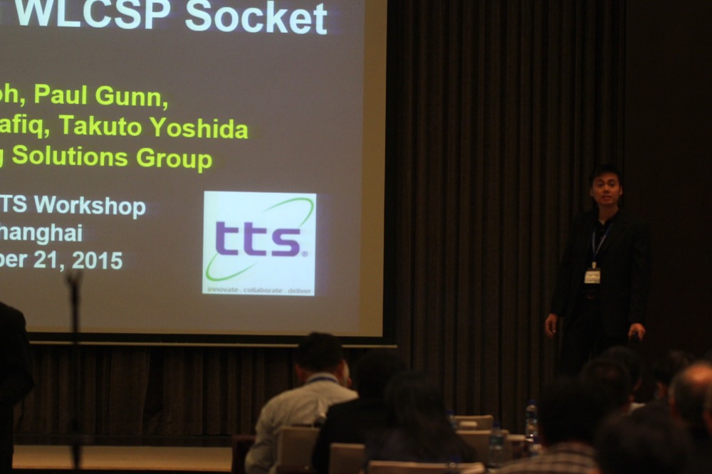
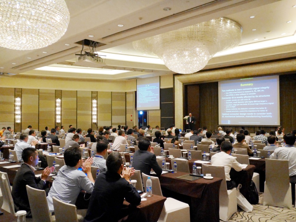
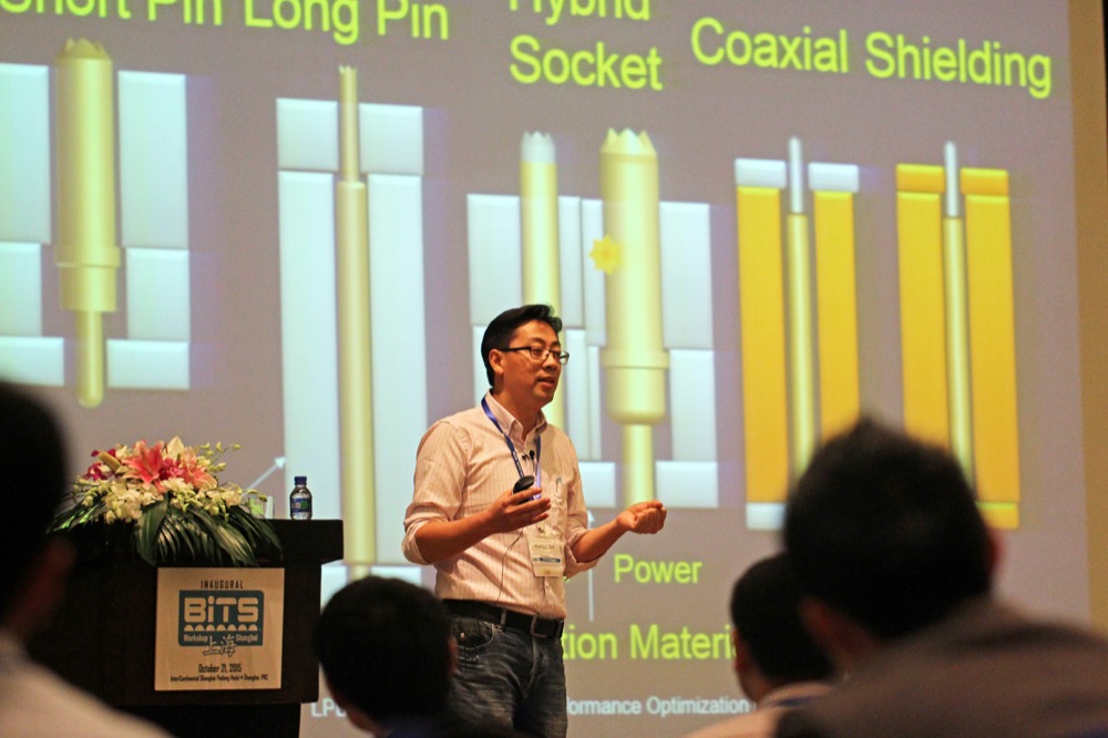
BiTS Shanghai will be a one day event featuring technical presentations highlighting the "Best of BiTS" along with new regional presentations. Learn what is Now & Next in burn-in and test of semiconductors!

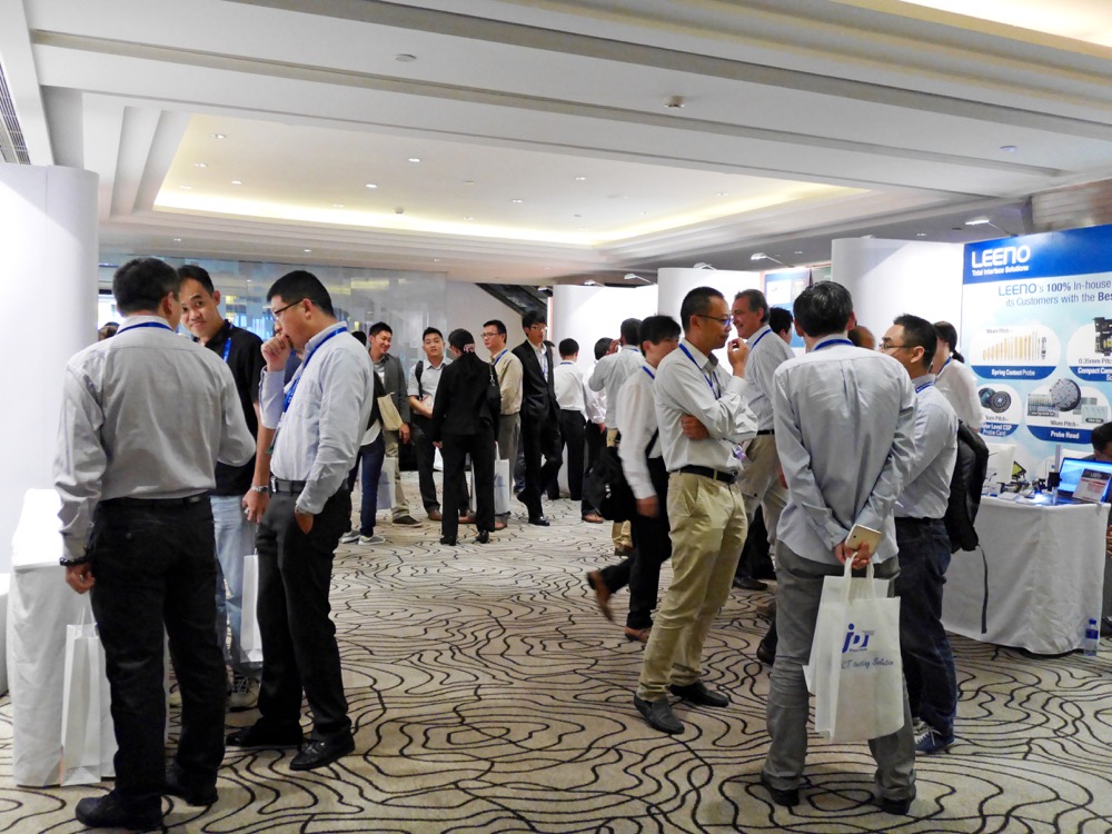
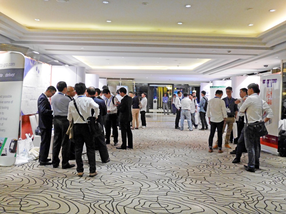
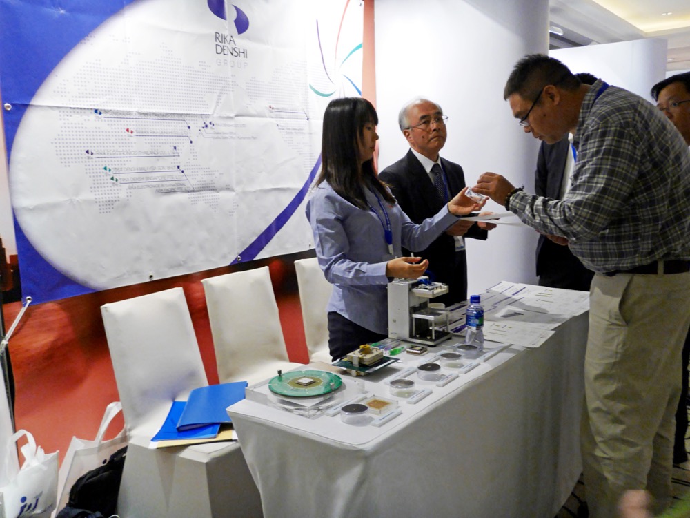
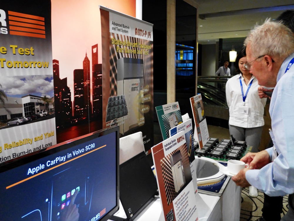
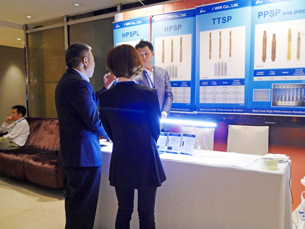
There will be a BiTS EXPO featuring international and local suppliers. This combined with great food will provide excellent opportunites for networking.

Welcome by Ira Feldman (Feldman Engineering), BiTS Workshop General Chair Keynote by Clements 'Ed' Pasua (PricewaterhouseCoopers) 'China's Impact on the Semiconductor Industry' Attentive audience at BiTS Jose Moreira (Advantest) Don Thompson (R&D Altanova) Appluading audience at BiTS Valts Treibergs (Xcerra Corporation) John West (VLSI Research Europe) Ira Feldman, BiTS Workshop General Chair Clark Liu (PowerTech Technology) Audience settling in before a presentation resumes One of the many great presentations at BiTS Audience listening intently to presenter Frank Zhou (Smiths Connectors), BiTS China Technical Program Committee Chair Audience applauding a well done presentation Yuanjun Shi (Twin Solution Technology), BiTS Chinal Technical Program Committee BiTS China Committee - Yuanjun Shi, Frank Zhou, Ira Feldman, Christine Zhu, Steven Zheng - not pictured: Takuto Yoshida, SL Wee, Tom Yin BiTS EXPO BiTS EXPO BiTS EXPO BiTS EXPO BiTS EXPO

BiTS Shanghai Archive 2015
Wednesday October 21, 2015
InterContinental Shanghai Pudong Hotel
No. 777 ZhangYang Road, Shanghai, 200120 China
9:00 - 9:15
Opening Remarks
Welcoming remarks from
Ira Feldman, BiTS Workshop General Chair, and
Steven Zheng, BiTS Shanghai Chair
> alt="Link to Opening Remarks">
9:15 - 10:00
Keynote Address
“China's Impact on the Semiconductor Industry”
alt="Ed Pausa">
Ed Pausa
Director
Technology Center
PricewaterhouseCoopers

“China's Impact on the Semiconductor Industry”
"主题:中国对半导体行业的影响"
Ed Pausa
PricewaterhouseCoopers

As Principal Author of PricewaterhouseCoopers’ “China’s Impact on the Semiconductor Industry – 2015 Update”, Mr. Pausa will provide an overview of China and the global semiconductor market. In particular, he will cover why and how China's semiconductor consumption has grown to represent more than half of the worldwide market for the last three years. Even though China’s semiconductor production has grown at a faster rate than consumption, China still only represents about 14% of worldwide output. What are the implications of China's ever-increasing integrated circuit (IC) consumption / production gap which reached a record $120bn in 2014?

Mr. Pausa has been an author of this annual PwC report for over a decade and has significant insight into the dynamics of the semiconductor market. The report is available at this link

作为“中国对半导体行业的影响-2015年更新版”的主撰写人,Pausa先生将综述中国和全球半导体市场的整体情况,并专注阐述在过去三年中中国的半导体消费为什么并如何成长为全球50%以上的庞大市场。虽然,中国半导体生产的增长超过了其消费的增长率,但是中国目前却只占有全球的14%产量。如何理解中国的急速增长的半导体芯片消费和生产能力之间的差距,这个差距在2014年已经达到历史高点的1200亿美金。

在过去10多年里,Pausa先生一直是这份PriceWaterhouseCoopers的年度报告的作者,并对半导体市场动态有非常独特的见解和洞察

Biography (English)

Ed Pausa

Ed Pausa has been associated with PricewaterhouseCoopers (PwC) for more than twenty years. An experienced multinational corporate executive, Mr. Pausa has more than 40 years of broad experience in the semiconductor industry. This includes 25 years’ experience at the corporate officer level in all four segments of the industry: integrated device manufacturer, semiconductor equipment and materials, semiconductor manufacturing services, and fabless semiconductor.

During his career he has directed 33 plants and subsidiary companies in 18 foreign countries and 11 plants in six states in the United States. In 1990 Mr. Pausa began his association with PwC when he started consulting with Coopers & Lybrand Managing Consulting Service after his retirement from National Semiconductor Corporation where he had served as Corporate Vice President of International Manufacturing and Services.

Mr. Pausa earned a Bachelor of Science Engineering with honors, a Master of Science in Metallurgy, and a graduate certificate in Business Management from the University of California at Berkeley. He holds the rank of Captain, United States Naval Reserve. PWC

Biography (Chinese)

Ed Pausa

Pausa先生在PriceWaterhousecoopers已经工作了20多年,是一位非常有经验的跨国公司高级管理人员。Pausa先生在半导体行业有40年以上的广泛经验,其中25年活跃在半导体行业的各个分属领域(包括integrated device manufacturer, semiconductor equipment and materials, semiconductor manufacturing services, and fabless semiconductor)。他曾经在18个国家管理过33个工厂和所属公司并在美国的6个州管理过11家工厂。在1990年,Pausa先生从National Semi的副总裁退休后,开始通过Coopers&Lybrand Managing Counsulting Service向PWC提供咨询服务

Pausa先生拥有工程荣誉学士学位,Metallurgy大学的科学硕士学位,以及加州大学Berkeley分校的管理学证书。他还是美国海军预备队的Captain军衔。

> alt="Link to Keynote video Pdf">
10:00 - 12:15
Session 1
Best of BiTS 2015
Awarding winning presentations from BiTS 2015
See updated versions of the top awarded presentations from the Burn-in & Test Strategies (BiTS) Workshop 2015 presented by the authors.

Technical presentations in English with bilingual question & answer period.

"PCB Test Fixture and DUT Socket Challenges for 32 Gbps/GBaud ATE Applications"
"超高速信号(32Gbps/Gbaud)的测试: 电路板与测试基座的设计与挑战"
Jose Moreira
Advantest
Christian Borelli
STMicroelectronics
Fulvio Corneo
STMicroelectronics
Abstract and Biography (English)

25 to 32 Gbps IO cells are now being integrated in large System on a Chip (SOC) integrated circuits for the wired communications market. This presents a challenge for the characterization and production testing of these devices using automated test equipment (ATE). One of the major challenges is the design of the PCB test fixture and especially the DUT socket due to the signal integrity challenges at the these high data rates. Even using an external loopback approach for IO testing, the test fixture and the DUT socket are critical because the signals on the loopback path run at-speed. In this paper we will discuss the challenges that 32 Gbps application present for PCB test fixture and socket design including the tradeoffs needed between characterization and manufacturing needs. We will also present some results obtained with a 32 Gbps capable ATE system where different standard socket technologies were evaluated. These measurements were performed with the socket as part of the final application environment and not as an individual component. The objective is to show how significant the socket impact is at these data rates. The authors main objective for this paper is to show these challenges from the end user point of view (IC Characterization and testing) to trigger the PCB and socket industry to further improve their socket technologies.

Jose Moreira

Jose Moreira is a senior staff engineer in the test cell innovation team of the SOC business unit at Advantest Boeblingen, Germany. He has a master of science in electrical and computer engineering from the Technical University of Lisbon and he is a senior member of the IEEE and member of the DesignCon technical committee. Jose has published multiple papers in several conferences and received several best paper awards at DesignCon and VOICE. He also has multiple submitted and awarded patents. He is co-author of the book "Testing High-Speed Interfaces with Automated Test Equipment" published by Artech House.

Abstract and Biography (Chinese)

有线通信市场使用的 SoC 芯片开始越来越多地集成 25~32 Gbps 的 IO 单元,这就给使用自动 测试设备(ATE)的产品性能测试与量产测试带来了挑战。主要的难点在于 PCB 测试治具的 设计,特别是被测品 Socket 的设计。高速数据传输下,信号完整度将有所损失,即使使用外 部回路的方法来进行 IO 测试,外部回路的信号传输速率也颇高,测试治具与被测品 socket 显得至关重要。由此,我们将讨论 32 Gbps 下 PCB 测试治具与 socket 设计所面临的挑战,包 括如果平衡产品性能与量产测试需求。我们还会展示兼容 32 Gbps 的自动测试设备(ATE) 系统的测试结果,各位可以看到使用不同 Socket 获得的测试结果差异。这些测试都是将 socket 融入整套测试环境而非作为单一对象测试来进行的,目的是对比 socket 对于高速数据 下测试的影响。作者希望从最终用户(芯片特性与测试)的角度为大家说明行业面临的挑战, 从而启迪 PCB 与 socket 行业相关人员进一步提高 socket 相关技术。

Jose Moreira

Jose Moreira 为德国 Advantest Boeblingen 公司 SoC 事业部测试创新小组的高级工程师。他毕 业于里斯本技术大学电气和计算机工程系,获得理科硕士学位,也是 IEEE 的 DesignCon 技术 委员会会员高级会员。Jose 曾在多个技术会议中发表薯片论文,曾荣获 DesignCon and VOICE 最佳论文奖。他还持有多个技术专利,为 Artech House 出版的《测试高速接口自动化测试设 备【Testing High‐Speed Interfaces with Automated Test Equipment】》一书的联合署名作者。

> alt="Link to Session 1 Paper 1">
-- Fifteen minute break --

"Designing Sockets for Ludicrous Speed (80 GHz)"
"适用于飞速(80 GHz)测试的 Socket 设计"
Don Thompson
R&D Altanova
Jose Moreira
Advantest
Abstract and Biography (English)

There are several new areas of the socket marketplace emerging where very high frequency sockets need to be developed. Two areas that look to become large volume producers of very high frequency parts are Near-field communication devices running at 59-66 Ghz and automotive radar running at around 76-81 GHz. Both are pushing socket performance and industry signal integrity skills far past their current levels. It is important that we as an industry make intelligent design decisions and understand how to test and measure sockets in this frequency class in order to support these new markets. This paper will do the following:

1. Present a guide for how to understand the performance of pins at these frequencies. The goal will be to focus on what's important for high frequency socket analysis and discount the pieces that aren't important.

2. Discuss the challenges and solutions for measuring a socket at these frequencies, tools required, calibration structures used, and discuss alternate options and why we selected the path we did. This will give a rational for the methodology and justify the accuracy of our results.

3. Review the measured results from our test structures, analyze results for success or failure and discuss our next steps toward development of a socket at these frequencies.

Don Thompson
Don Thompson spent 11 years at Teradyne developing interfaces for their latest generation of their Automated Test Equipment including 3 years at Teradyne Japan working on high speed SERDES instruments. Don is the manager of R&D Altanova's design group and works on all things Signal Integrity and Power Integrity that are related to cutting edge load board designs. He presents at industry conferences regularly and won Best Presentation at BITS workshop in 2014.

Abstract and Biography (Chinese)

新兴 Socket 市场主要关注高频 socket 研发,其中有几个新兴领域特别值得关注,其中预计 市场容量最大的两块分别是可在 59‐66 Ghz 下运行的近地通信设备(NFC),以及可在 76‐81 GHz 下运行的汽车雷达设备。两者都在极大程度上推动着现有 socket 性能与信号完整度技 术水平的快速提升。由此,我们作为一个行业整体需要做出明智的设计决策,并理解如何在 这个频率级上对 socket 进行测试测量以支持这些新兴市场,这一点非常重要。

本文主要包含以下几点:

1. 帮助各位理解这些高频级下的 pin 针性能。去芜存菁,主要关注高频 socket 分析要点。.

2. 讨论这些高频级下 socket 测试测量的难点与解决方案,需要何种工具,使用的校准结构, 备选方案,以及为何选择某条通路。由此,届时我们所用方法的合理性与测试结果的准确程 度。

3. 回顾使用这些测试结构的测试结果,分析成功或失效的结果,并讨论这些高频 socket 的 进一步研发方向。

Don Thompson
Don Thompson在Teradyne公司已工作超过11年,负责开发了最新一代自动测试设备(ATE), 并在 Teradyne 日本 分公司负责过高速 SERDES 设备研发项目。Don 为 R&D Altanova 研发组经理,曾负责 Signal Integrity and PowerIntegrity 所有关于前沿线路板的设计研发工作。他曾多次定期在行业大会 上发表论文,并获得 BiTS Workshop 2014 最佳演讲大奖。

> alt="Link to Session 1 Paper 2">

"Comparison of Different Methods in Determining Current Carrying Capacity of Semiconductor Test Contacts"
"半导体测试触头电流承载能力测定方法的比较"
Valts Treibergs
Xcerra Corporation
Mitchell Nelson
Xcerra Corporation
Abstract and Biography (English)


As has been pointed out by various presenters at BiTS, there is no one consistent method for measuring, determining, and specifying Current Carrying Capacity (CCC) in test socket interconnects. This presentation will review existing test methods and compare advantages and disadvantages of each method. The bulk of the focus will be on a detailed comparison of the thermocouple-based T-rise method vs. the force relaxation method (ISMI). Data will be presented using both methods on the same spring probe contact system and compared. Data should support one of these methods as a best practice. Other methods, such as infrared imaging, will briefly be discussed as well. I hope the talk will stimulate a technical discussion, and ultimately move to a consensus in the socket manufacturer and socket user community in the way CCC is tested and specified.

Valts Treibergs
Valts Treibergs has 25 years experience developing semiconductor and high-speed interconnects. He has presented at BiTS numerous times, and has authored a number of articles in various industry publications. Valts holds 10 patents, and is a graduate of the University of Minnesota, and currently is R&D Engineering Manager at Xcerra Corporation in Minnesota.

Abstract and Biography (Chinese)


正如 BiTS 大会多位演讲人指出,针对电流承载能力(CCC),测试 socket 触头并没有唯一不 变的测量,判定和标准化的方法。此篇演讲旨在回顾现有的测试方法,对每种方法的优劣势 进行比较。论文主要篇幅讨论了基于热电偶的 T‐rise 法与力松弛法(ISMI)细致对比,实验 使用了同一套弹簧探针接触系统,呈现并对比了测试结果数据,并由此获得一套最佳的测试 方法。同时,本文也会对其他测试方法,例如红外成像,进行简要讨论。我希望这次演讲与 对话能够激发又一轮的技术讨论,并最终推动 socket 厂商与用户群体就电流承载能力(CCC) 测试方法与标准达成一致。

Valts Treibergs
Valts Treibergs 在半导体与高速连接器的研发领域拥有 25 年专业经验,曾多次在 BiTS 大会发 表技术论文,并多次在各种行业期刊上发表文章。Valts 拥有 10 项专利,毕业于明尼苏达大 学,目前在 Xcerra Corporation 公司任研发工程经理。

> alt="Link to Session 1 Paper 3">

"The Economics of Semiconductor Test – Challenges and Opportunities for 2016"
"半导体测试的经济学-2016年的挑战和机遇"
John West
VLSI Research Europe
Abstract and Biography (English)


Growth in semiconductor sales has been slowing since the middle of 2014 and is now entering negative territory. It is not surprising that, as revenues have been falling, chipmakers are pressuring their test equipment and service suppliers to reduce costs. This is a particular problem as the cost of test for testing leading edge devices has been outstripping the growth in semiconductor revenues. These advanced devices will only get harder to test in the future and cost effective solutions have yet to be found. This presentation reviews the current market situation and highlights the areas where growing costs are causing most concern.

John West
John West is Managing Director of VLSI Research Europe and is responsible for supporting all of VLSI Research’s European activities. In addition, he developed the Critical Subsystems Market service in 2001 and more recently has been the principal analyst for VLSI’s Test Consumables reports. He is the author of numerous proprietary market research reports. He was awarded an MBA from Cranfield University and has a degree in Medical Physics from the University of London.

Abstract and Biography (Chinese)


半导体产业销售的增长自从2014年中期就开始减缓,现在更是要进入了负增长的局面。通常情况下,当盈利降低时,芯片制造商会给提供测试设备和相关服务的供应商施以价格方面的压力。当测试顶尖设备的价格超出半导体收益的增长时,这种问题就尤为突显。所以领先设备的测试在未来会变得越来越难,并且成本效益的解决方法还有待发现。 这次演讲将会回顾当前半导体测试产业的市场状况并且着重介绍持续增长的费用会在哪些领域引起最大的关注。

John West
John West是VLSI Research Europe的总经理,负责管理VLSI Research所有在欧洲的事务。他在2001年开发出了半导体产业中的关键子系统的市场服务,他也是最近VLSI Research发布的测试耗材报告的首席分析师。 John同时也是众多专有市场研究报告的作者。John拥有英国克兰菲尔德大学MBA硕士学位和伦敦大学的医学物理学位。

> alt="Link to Session 1 Paper 4">
12:15 - 14:15
Lunch &
BiTS EXPO
BiTS EXPO OPENS
Enjoy the delicious hot buffet lunch and networking time. Then take the time to explore the BiTS EXPO. There will be many great exhibits to explore what is Now & Next in the test and burn-in of semiconductors. You will be certain to see something new or meet someone new.

As attendees to BiTS know, there is always excellent food, drinks, and time for attendees to network with exhibitors!

BiTS EXPO will be remain open throughout the afternoon until 18:00

14:15 - 16:15
Session 2
East Meets West
Asian BiTS Papers
Hear up-to-date local presentations from across Asia describing semiconductor test and burn-in challenges. These regional and global experts will share their expertise and solutions to these challenges.

Technical presentations in Chinese or English as noted. Slides in English with bilingual question & answer period.

"WLP Probing Technology Opportunity and Challenge"
"WLP探测技术的机会与挑战"
Clark Liu
PowerTech Technology Inc.
Abstract and Biography (English)

WLP (Wafer Level Package) technology is being rapidly deployed by increasing end user application volumes. WLP probing technology as a manufacturing test process needs to achieve the targets of yield, cost and performance. There has been many presentations on this topic at recent conferences including BiTS 2015 and Semiconductor Wafer Test Workshop (SWTW) 2015. This intense focus is due to the unmeet needs of the technology and customer requirements that keep pushing the probing and test industry harder. This presentation will introduce the topics of WLP probing technology, the opportunities, and the challenges. From probing technology required for WLP process technology to probe card lead times and topics in between that will drive this market will be reviewed.

Clark Liu
Clark current is Director of Chip Probing Division, PowerTech Technology Inc., Taiwan and he is a SWTW committee member. He has Master of Engineering management from Tsing Hua University at Taiwan. Clark has over 20 years experience in the semiconductor testing industry. He had lead the development, with key suppliers worldwide, of 300 mm wafer probing technology starting in 1998. He also has multiple submitted and awarded patents. Now Clark’s major focus is on WLP probing technology and business.

Abstract and Biography (Chinese)

WLP(晶圆级封装)技术的发展推动最终用户应用.WLP探测技术的制造工艺,以确定测试结果与产量,成本和性能目标匹配。今年 SWTW,有几篇文章围绕这一主题,不断探索推动行业不断发展的新技术,以满足客户的需求。 本文将介绍2015年 SWTW涉及WLP的探测技术的机会与挑战主题。从探测技术落后的WLP工艺技术和探测卡的准备时间会尽快处理测头卡行业。

Clark Liu
Clark Liu 目前是台湾力成科技有限公司芯片探测处的处长,他是 SWTW委员会。他拥有台湾清华大学工程管理硕士学位。Clark为半导体测试产业有超过20年的经验。他从1998年发展与世界上主要供应商为300mm晶圆探测技术,他还多次提交并获得专利。现在,他主要专注于WLP探测技术和业务。

> alt="Link to Session 2 Paper 1">

"Pushing the Envelope in DFM (Design for Manufacturing) for 0.2mm Pitch WLCSP Socket"
"研发和改进WLCSP Socket, 0.2mm 微间距晶圆测试插座的设计与制造."
Colin Koh
Test Tooling Solutions Group
Abstract and Biography (English)

The WLCSP (Wafer Level Chip Scale Packaging) test socket is designed on 0.2mm pitch MTS (Multi Test Site) socket. However an excellent design cannot be done only by current experience and knowledge. We hope to share the difficulty and the coping process that we experienced from design to fabrication. We faced a problem on socket warpage by mismatch of warpage simulation and actual measurement. We solved the problem by improving simulation method and socket design. This presentation will highlight how we have pushed the envelope in DFM (Design for Manufacturing) for 0.2mm Pitch WLCSP Socket.

Colin Koh
Colin Koh received his Diploma in Engineering (Mechatronics) from Ngee Ann Polytechnic and a Bachelor of Business & Commerce from Monash University. He is a Sales Manager at Test Tooling Solutions Group in Singapore.

Abstract and Biography (Chinese)

WLCSP 测试插座是专门为0.2mm 微间距晶圆测试的需求而研发的. 并保持可同时测试多组晶圆为原则. 在研发及制造的过程中, 曾经面临无数次的困难与挑战, 经过多次设计上的改良和摸拟实验, 终于达到成功的结果. 在本次的发表会上, 我们将与您分享 WLCSP 测试插座的研发历程与结果.

Colin Koh
Test Tooling Solutions 业务经理 拥有机械工程及商务贸易学位

> alt="Link to Session 2 Paper 2">

"Signal Integrity & Impacts by Connector Structures"
"芯片测试探针/座的信号完整性 及其影响"
Jiachun (Frank) Zhou
Smiths Connectors
Dexian Liu
Smiths Connectors
Professor Sun Ling
Jiangsu Key Lab of ASIC Design, Nantong University
Abstract and Biography (English)

The signal integrity (SI or RF) characteristics of test socket or connectors is one of key performances concerned in package testing, especially for high frequency device testing. Due to its complexity, the basic theory of SI and its correlations to test socket/connectors structures are not fully understood. Over years, lots of efforts have been spent in this field, including measurement methods, simulations, and studies on correlations of connector structures to their signal integrity performance. This paper will provide the audience with basic knowledge, test/simulation methodologies, and connector selections based on signal integrity requirements. Below are the outlines:

1. Signal integrity basics will cover: Insertion Loss; Return Loss; Bandwidth; Impedance; Cross Talk; Single Ended and Differential.

2. Signal integrity simulations and measurement methodology Signal simulations software and out puts Measurement set up & basic methodology

3. Impacts of contactor structures on SI: Contactor length; Field vs. edge; Pitch or connector diameter Socket material Coaxial & impedance control structure

As a summary, audience can have a clear picture of signal integrity technical specifications, measurements methods, simulation, and considerations in selecting test socket/connector based on signal integrity.

Jiachun Zhou (Frank), PhD
Frank has worked in Semiconductor test equipment and contactor industry over 15 years. He has developed new contactor technologies & products and is a major contributor for the test socket & spring probe business. Frank manages global Semi engineering group in US & Asia for Smiths Connectors. Prior the semiconductor industry. he was involved with renewable energy research. Frank has over 20 patents in semiconductor connector related products & technologies, and over 50 publications in journal & international conferences Frank has a Ph.D. in Mechanical Engineering & Material Science from the University of Hawaii, 1998.

Abstract and Biography (Chinese)

测试 socket 及连接器的信号完整度(SI 或 RF)特性,是封装测试的重要指标,对于高频器 件测试尤为重要。由于测试复杂度高,SI 及其与测试 Socket、连接器结构的相关性方面的基 础理论还不完善。多年来,行业在此方面做了大量研究,包括测量方法,仿真,以及连接器 结构对其信号完整度的影响研究。这篇演讲将为听众普及这方面的基础知识,测试/ 仿真方 法,如何基于信号完整度要求选择连接器,以下为大纲:

1. 信号完整度包括:插入损耗;回波损耗;带宽;阻抗;串扰;单端和差分。

2. 信号完整度仿真及测试测量方法:信号仿真软件与输出测量装置及基本方法

3. 触头结构对信号完整度的影响:触头长度;磁场 vs.边缘;间距或连接器直径的承插材料 同轴阻抗控制结构

总而言之,听众基本可以明确信号完整性的技术规格,测量方法,仿真和如何基于信号完整 度来选择测试 socket/连接器。

Jiachun Zhou (Frank), PhD
Frank Zhou 在半导体测试设备与连接器行业拥有超过 15 年的专业经验,曾负责多个新连接 器技术与产品等的研发,并未测试 socket 及探针行业做出了巨大贡献,负责管理 Smiths Connectors 美国与亚洲的全球半导体工程组。在加入半导体行业之前,Frank 曾主攻可再生 能源研究。他在半导体连接器领域拥有 20 项与产品及技术相关专利,并在行业期刊及国际 会议上发布超过 50 篇论文。Frank 于 1998 年毕业于夏威夷大学,拥有机械工程与材料科学 博士学位。

> alt="Link to Session 2 Paper 3">

"LPDDR4 Signal & Power Performance Optimization By Hardware"
"通过测试硬件的优化来提升LPDDR4信号和电源的性能" alt="Ribbon for best Paper">
Yuanjun Shi
Twinsolution Technology
Xiao Yao
HiSilicon Technologies Co
Abstract and Biography (English)

A high speed interconnectors for LPDDR4 using optimized spring pin by modeling, testing and measuring was implemented. In the real testing environment signal intrusion and power supply noise are serious challenges and have to be carefully optimized to meet the data rate, and other chip parameters target. Spring pin inductance has bigger impact to jitter performance as well as simultaneous switching output (SSO) noise in the full chain system. This paper shows how to analyze and minimize SI, Cross Talk, Jitter, and SSO by optimize different spring pin as well as improve the performance of mechanical structures for the LPDDR4 test interface.

Yuanjun Shi

Yuanjun Shi is currently R&D manager of Twinsolution Technology Shanghai INC., He has Bachelor Degree of electronic engineering from Suzhou University and MBA from Victoria University Switzerland. Yuanjun has over 15 years’ experience in the semiconductor industry. Now Yuan Jun’s major focus is on developing high quality metal contactors.

Abstract and Biography (Chinese)

介绍一种通过建模仿真和测试相结合来提升LPDDR4的测试性能的方法。在实际测试过程中信号干扰,以及电源噪音是非常严重的挑战,不过我们可以通优化连接器的选型和设计来达到测试的预期值。连接探针的电感对Jitter和SSO噪音影响非常大。这篇文章将介绍如何分析和优化SI, Cross Talk, Jitter, SSO以及部分的机械性能优化。

Yuanjun Shi

施 元军目前是上 海韬盛电子科技股份有限公司的研发经理。他在半导体测试产业有超过15年 的经验,并致力于测试连接器对信号和电源完整性影响研究多年,他还多次提交并获得专利。其中以高 隔离度的测试插座的研发最具代表性。现在他主要专注于开发低接触电阻和长寿命的金属接触探针。

> alt="Link to Session 2 Paper 4">
16:15 - 18:00
BiTS EXPO
& Afternoon Tea
BiTS EXPO Continues
Enjoy additional time to meet with the presenters, network, and explore the BiTS EXPO further. There will be many great exhibits to explore what is Now & Next in the test and burn-in of semiconductors.

Afternoon refreshments will be served.