BiTS 2015 Archive Program

The Burn-in and Test Strategies (BiTS) Workshop successfully held its sixteenth annual event in Mesa, Arizona on March 15-18, 2015. Throughout the three-day event, attendees participated in a hands-on tutorial, a keynote address from Joe Bruen of Freescale Semiconductor, and an invited talk from Brandon Prior of Prismark Partners as well as technical content from industry experts and participants. Heidi Barnes of Keysight Technologies lead the hands-on tutorial, “How to Make a High Frequency Transparent Socket”, which preceded the three-day workshop.

Twenty-nine technical papers in eight sessions plus five posters in the poster session covered topical areas as diverse as test and socket solutions for testing automotive radar devices, device reliability, and test solutions for both WLCSP and MEMS devices.

BiTS Workshop, which is the premier industry event focused on the burn-in and test of packaged semiconductors, drew more than 350 attendees. Fabless and integrated device manufacturers as well as companies from the supply chain delivering burn-in, test, and test consumable products were well represented. More than forty percent of attendees were from international locations. An important component of the workshop has long been the BiTS EXPO, which is open to not only conference attendees but industry and academic members of the community. BiTS EXPO displays featured the latest products and services further adding to the valuable insights and data about what is Now & Next in burn-in and test shared at BiTS.

Market outlooks were delivered by representatives of Feldman Engineering and VLSI Research. Opportunities for networking and social activities rounded out the 2015 event.

BiTS EXPO 2015

An international gathering of exhibitors from test and burn-in related industries showed what is
Now & Next in equipment, materials, and consummables during the BiTS EXPO.
Please thank the BiTS 2015 EXPO exhibitors.

Check out all the excitement this year at BiTS EXPO 2015!


Distinguished and Keynote Speaker Interviews

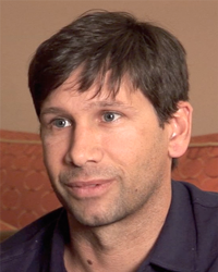
A peek into the mind of our distinguished speaker Brandon Prior at BiTS 2015.


Hear our keynote speaker Joe Bruen discuss future trends at BiTS 2015.


BiTS 2015 Principal Sponsors

The BiTS Workshop would like to thank our principal sponsors for their continuing support of the workshop.

Tutorial Day
Sunday March 15, 2015
noon - 6:00 PM
Tutorial
How to Make a High Frequency Transparent Socket
A hands-on workshop to learn the Signal Integrity (SI) basics of simulation and measurement techniques for test sockets.
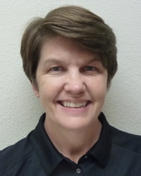
Heidi Barnes
Heidi Barnes
Senior Application Engineer
Keysight Technologies
The ideal transparent socket would make us millions if we could actually find it, but in the real world we cannot simply time travel between two points and ignore what is in the middle. At DC the focus is on the contact resistance, but at the high frequencies of multi-gigabit interconnects one can be plagued by additional dielectric loss, reflections, and complicated multi-mode resonances. This means that if your socket is not working as required at 8, 16, 28 or 40 Gbps then that classic voltmeter sitting on the test bench is not going to do the job. Signal Integrity expert, Dr. Eric Bogatin, emphasizes that a good engineering practice is to always have models or simulations to predict the outcome of a measurement. Often there is a large void between the too simple V=IR calculation and the too complicated full 3D-EM simulation with Maxwell’s equations. Engineers confronted with these two options will typically do nothing on the simulation side and then just point to the data sheet.

A better option is to explore the power of simple transmission line theory and network analysis with scattering parameters (S-Parameters). Simple deconstructed transmission line models can be used in simulations to quickly evaluate the impact of resistance, dielectric loss, reflections, and even resonances. The results of the simulations provide valuable insights into how transparent a socket is for your application. Using hands-on computer labs with both frequency domain and time domain simulations attendees at the workshop will be able to test out their ability to debug a failed test socket measurement and get a socket design that is transparent for an 8.4 Gbps PCIe application example. These simple deconstructed transmission line models also improve the effectiveness of full 3D-EM simulations. Knowing what to expect from the EM simulation insures better setup of the stimulus ports, and effective use of simplification trade-offs.

Another way to make a transparent socket is to mathematically remove its effects from the measurement. This can be a simple calibration of removing a static IR drop at DC, but at high frequencies one must calibrate out both the “attenuation” drop and the interaction of reflected signals. To make things even more complicated, one must also keep track of the phase relationship between the current and voltages at high frequencies. Simple transmission line theory and network analysis scattering parameters (S-parameters) do just that, and with a bit of matrix math they can remove the effects of the socket fixture from a measurement. The signal integrity world calls this fixture de-embedding. Using hands-on computer labs and actual test equipment hardware attendees will learn how to measure socket fixture S-parameters using a two-tier Short/Open/Load/Through (SOLT) with 2-port probing or 1-port open calibration techniques. The socket fixture S-parameters can then be used in the time domain to remove the effects of the socket fixture from the measurement making the socket transparent. This sounds too good to be true, and so again one can turn to simulation to see where it can go wrong and get a practical understanding of how and when to implement fixture de-embedding.

The goal of this half-day tutorial is to give the attendees a toolbox of both simulation and measurement signal integrity techniques for characterizing a socket and ways to make it transparent for high frequency multi-gigabit applications.

Note: Due to the hands-on nature of this Tutorial, attendance will be limited. Please sign-up early to not miss out!

Ms. Heidi Barnes is a Senior Application Engineer for High Speed Digital applications in the EEsof EDA Group of Keysight Technologies, a spin-off of Agilent Technologies. Past experience includes over 6 years in signal integrity for ATE test fixtures for Verigy, an Advantest Group, and 6 years in RF/Microwave microcircuit packaging for Agilent Technologies. She rejoined Agilent Technologies in 2012, and holds a Bachelor of Science degree in electrical engineering from the California Institute of Technology.
Link to tutorial video and Pdf
8:30 - 9:30 PM
Distinguished Speaker
Small Form Factor Package Trends to 2020
Heidi Barnes
Brandon Prior
Senior Consultant
Prismark Partners
Mr. Prior will share an overview of the global packaging market. His presentation will focus on the impact and growth of small form factor packages such as multi-row QFN, WLCSP, Fan-Out WLCSP and MIS BGA on the electronics industry infrastructure. Teardowns of products from early adopters such as Apple, Samsung, Huawei, and Xiaomi will be used to highlight how fast this change is occurring.
Mr. Prior is a Senior Consultant at Prismark Partners. He joined Prismark in 1996 and is the author of their Semiconductor and Packaging Report.In his role at Prismark, he provides market and competitive analyses within semiconductor packaging and interconnects.
Link to tutorial video and Pdf
Frontiers Day
Monday March 16, 2015
8:30 - 9:00 AM
Opening Remarks
Welcoming remarks from the General Chair, Ira Feldman
Link to tutorial video and Pdf
9:00 - 10:00 AM
Keynote Address
Making Sense of the Internet of Tomorrow
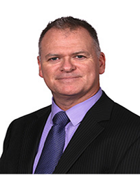
Joe Bruen
Joe Bruen
Director of Product Improvement &
Operations
Sensor Solutions Division
Freescale Semiconductor
Mr. Joe Bruen will share his thoughts on microelectromechanical systems (MEMS) sensing technology and the end applications which include automobiles to smartphones and everything in between. He will explore the Internet of Things (IoT) which will connect all these devices and will become the Internet of Tomorrow.

Mr. Joe Bruen is Director of Product Improvement and Operations in the Sensor Solutions Division for Freescale Semiconductor.Past experiences include twenty-seven years of increasing responsibilities in manufacturing, planning, finance, and operations having started earlier in his career at Motorola which is now Freescale.He holds a Graduate in Business degree from Glasgow Caledonian University.


Link to tutorial video and Pdf
10:30 AM - 12:30 PM
Session 1
Putting MEMS to the Test
Testing MEMS Devices
With microelectromechanical systems (MEMS) devices in consumer products becoming as common as parades on St. Patrick’s Day, reducing the cost of test is more important than ever. It is no wonder the MEMS test session addresses lowering the cost of MEMS test. John Rychik, Xcerra, describes various approaches to reduce the cost of calibration and test through test cell integration. Vesa Hentonnen, Afore, covers three ways to decrease the cost of test to less than one cent. These are parallelism, shortening the process, and choice of tester. Wendy Chen, KYEC, explains a cost effective test strategy achieved by adding built-in-self test (BIST) and built-in self-calibration (BISC). These design-for-test methods can be applied to MEMS devices by integrating a single CMOS die or through 3D stacked die integration. The session closes with Peter Jones, Freescale, discussing a novel method for performing stress tests on MEMS die-form pressure sensors.
Link to tutorial video and Pdf
"'Taking MEMS Test and Calibration to the Next Level' - An Integrated Platform Approach Driving Further MEMS Growth"
John Rychcik
Xcerra Corporation
"The Target for Consumer MEMS Testing Should Be Under 1 Cent Level"
Vesa Henttonen
Afore Oy
"MEMS IC Manufacturing Test Cost Effective Strategies"
Wendy Chen
KYEC
Andrei Berar
KYEC
"BURst Pressure (BURP) Stress Test for MEMS Pressure Sensors"
Ribbon for Attendee Choice
Peter Jones
Freescale Semiconductor
Ray Sessego
Freescale Semiconductor
1:30 PM - 3:30 PM
Session 2
Spanning the Socket Rainbow
Test Socket Applications
Test socket solutions and the requirements of the device under test (DUT) vary according to the device end application. This session spans the socket spectrum from automotive applications, which require devices to withstand extreme temperature and high current, to mobile applications, which have high cost sensitivity. Markus Wagner, Cohu, explores contacting solutions for high power bare die testing. Valts Treibergs, Xcerra, compares different methods for determining current carrying capacity in test socket interconnects. Andreas Nagy, Xcerra, gives an overview of test temperature requirements of automotive and consumer applications and discusses consequences for test strategies. Praveen kumar Ramamoorthy, Infineon, focuses on socket design and development specifically for the extreme temperature and high current testing challenges of automotive devices.
Link to tutorial video and Pdf
"Contacting Solutions for High Power Bare Die Testing (IGBT MOS-FET and Diodes)"
Markus Wagner
Cohu SEG
"Comparison of Different Methods in Determining Current Carrying Capacity of Semiconductor Test Contacts"
Ribbon for best Tutorial
Valts Treibergs
Xcerra Corporation
"Extreme Temperature and High Current Testing Challenges of Automotive Devices"
Praveen kumar Ramamoorthy
Infineon Technologies
Dan Maccoux
JF Microtechnology SDN BHD
Muhamad Izzat bin Roslee
JF Microtechnology Berhad
Murad Hudda
Infineon Technologies
"Are New Temperature Test Strategies Needed? Meeting Performance and Cost Requirements of Today’s Applications"
Andreas Nagy
Xcerra Corporation
3:30 PM - 4:30 PM
Poster Session
Break & Networking
Poster Sessions are a great way to network through interaction with the poster presenters and other curious bystanders. At the same time enjoy the break refreshments and networking.
Link to tutorial video and Pdf
"HVM Solution for System Validation with OEM Socket"
Shaul Lupo
Intel
"Kelvin Contact Solution for WLCSP"
Ribbon for best Poster
Jay Kim
Leeno Industrial Inc.
Daniel Shin
Leeno Industrial Inc.
"Impact of Oxidation on Elastomer Contact"
Ila Pal
Ironwood Electronics
"The Next Generation of Scrub Contacting Technology"
Bert Brost
Multitest, Xcerra
Tony Tiengtum
Multitest, Xcerra
"Laser Cleaning vs Brush Cleaning"
J.M. Lee
IMT Co. Ltd.
J.B. Kim
IMT Co. Ltd.
H.W. Moon
IMT Co. Ltd.
D.S. Kim
Amkor Technology Co.
C.H. Jung
Amkor Technology Co.
4:30 PM - 6:00 PM
Session 3
Wafer Level Pots of Gold
Wafer Level Chip Scale Packaging (WLCSP)
Wafer level chip scale packages (WLCSP) are all the rage, and testing them is becoming easier and more cost effective as new probe technologies and probe card designs become available. This session explores four newly developed test solutions for WLCSP. Frank Zhou, Smiths Connectors, presents a tip co-planarity analysis of a 200 µm pitch spring probe head for WLCSP. Zhou describes the structure of the probe head and spring contact probes along with key features and their impacts on co-planarity of probe head contactor tips. Paul Gunn, Test Tooling Solutions Group, reports on design for manufacturing (DFM) efforts in the development of a 0.2mm WLCSP test socket. Khaled Elmadbouly, Smiths Connectors, discusses the challenges of building fan-out printed circuit boards (PCB) for use as space transformers in probe heads for multi-site WLCSP with pitches greater than 0.2 mm.
Link to tutorial video and Pdf
"Coplanarity Analysis of WLCSP Spring Probe Head"
Jiachun (Frank) Zhou
Smiths Connectors
Daniel DelVecchio
Smiths Connectors
Cody Jacob
Smiths Connectors
"Pushing the envelope in DFM (Design for Manufacturing) for 0.2 mm Pitch WLCSP Socket"
Paul Gunn
Test Tooling Solutions Group
Muhammad Syafiq
Test Tooling Solutions Group
Takuto Yoshida
Test Tooling Solutions Group
"Space Transformer PCB For Testing 200 µm WLCSP"
Khaled Elmadbouly
Smiths Connectors
6:00 - 9:00 PM
BiTS EXPO &
Reception
The BiTS EXPO is a very popular part of the BiTS program with many great exhibits to explore what is Now & Next in the test and burn-in of packaged semiconductors. There is always something new to see or someone new to meet. Not to mention excellent food, drinks, and time for attendees to network with exhibitors!
Performance Day
Tuesday March 17, 2015
8:00 - 10:00 AM
Session 4
Material Magic
Materials and fabrication processes
Contacts, test probes, and sockets have to accommodate ever-finer pitches, while holding up repeatedly to increasingly stressful conditions. This session looks at the impact of choosing the right materials and fabrication processes to address these situations and to increase the life of test consumables. Mike Gideon, Materion, discusses reliability and failure over time along with how to prevent failure by understanding root causes. Jimmy Johnson, Tyco Electronics, investigates using cold heading technology, selective gold plating, and a proprietary plating process to produce lower cost, high-reliability burn-in and test sockets. Jeb Flemming, 3D Glass Solutions, explores glass as an alternative to injected molded plastic for cost-effective test and burn-in sockets for radio-frequency (RF) device test. Bert Brost, Xcerra, talks about a novel coating technology that prevents solder migration at the contactor tips, thereby improving contact stability.
Link to tutorial video and Pdf
"Reliability and Failure over Time"
Mike Gedeon
Materion
"Using Cold Heading Technology and Deutsch Coat to Produce Test Probes & Spring Contacts "
Jimmy L. Johnson
Tyco Electronics
"APEX Glass for Burn-In and Test Sockets"
Ribbon for best Tutorial
Jeb H. Flemming
3D Glass Solutions, Inc.
Tim Foster
3D Glass Solutions, Inc.
"C3 Coating : Solution for IC Testing"
Bert Brost
Xcerra Corporation
Valts Treibergs
Xcerra Corporation
Nakaya Katsura
Kobelco Research Institute, Inc.
10:30 AM - 12:30 PM
Session 5
Handle With Care
Test Cell Integration
Test cell integration is best not left to the “luck o’ the Irish.” Testing today’s packaged semiconductor devices requires careful integration of automated test equipment (ATE) and handlers to reduce the cost of test. In this first of two sessions, presenters examine ways to streamline processes as well as alternative approaches that reduce the need for costly ATE and handlers. Alexander Wieler, esmo, starts with a semi-automated device interface board (DIB) loader, which allows for the quick exchange of DIBs without undocking the tester from the handler. Raimondo Sessego, Freescale, introduces a novel approach to testing MEMS G Cell devices. Stanley explains how this mechanical-flip burn-in system for tire pressure monitoring system (TPMS) sensors eliminates the need for a high cost ATE and flip handler combination. Mike Frazier, Xcerra, reviews the challenges of testing and handling singulated WLCSP devices using a strip or carrier format.
Link to tutorial video and Pdf
"Semi Automated DIB/PIB Loader"
Alexander Wieler
esmo AG
"Mechanical Flip Burn In (FBI) for Tire Pressure Monitoring System"
Raimondo Sessego
Freescale Semiconductor
James Stanley
Freescale Semiconductor
Joe Milazzo
Freescale Semiconductor
"Final Test Solution of WLCSP devices"
Mike Frazier
Xcerra Corporation
1:30 - 3:30 PM
Session 6
Lord of the Dance
Simulation & Performance
Simulation and modeling of performance is one of the most crucial design tasks for developing test hardware. It is essential to ensure the highest possible performance from wafer probes, sockets, contactors, and printed circuit boards. Mohammed Eldessouki, SV Probe, details the importance of implementing electrical performance simulation of the probe head on a semiconductor wafer probe card using SPICE based simulators. Gert Hohenwarter, GateWave Northern, reviews characterization and use of Kelvin sockets at RF frequencies. He explains that the proper design and analysis of the test environment requires knowledge of the input and output parameters of the DUT. Don Thompson, R&D Altanova, discusses measuring a socket at very high frequencies and the rational for this methodology. Jose Moreira, Advantest, reviews a 32 Gbps application that presents challenges for PCB test fixture and socket design. Jose describes the ATE system measurements results and improvements required.
Link to tutorial video and Pdf
"Electrical circuit model for silicon wafer spring pin probe"
Mohamed Eldessouki
SV Probe
"Kelvin Sockets at Speed"
Gert Hohenwarter
GateWave Northern, Inc.
"Designing Sockets for Ludicrous Speed (80 GHz)"
Ribbon for best Paper
Don Thompson
R&D Altanova
Jose Moreira
Advantest
"PCB Test Fixture and DUT Socket Challenges for 32 Gbps/GBaud ATE Applications"
Ribbon for best Tutorial
Jose Moreira
Advantest
Christian Borelli
STMicroelectronics
Fulvio Corneo
STMicroelectronics
3:30 - 6:30 PM
BiTS EXPO
Continue to explore the great exhibits at the BiTS EXPO to see what is Now & Next in the test and burn-in of packaged semiconductors. There is always something new to see or someone new to meet. Refreshments and drinks are served but don't spoil your appetitute before the BiTS Social...
6:30 - 9:30 PM
BiTS Social Event
Celebrate St. Patrick's Day
Don't miss the BiTS celebration of St. Patrick's Day! There will be plenty of excellent food and drink inspired by the holiday with a twist. And you'll get to try your luck in the BiTS Casino!
Solutions Day
Wednesday March 18, 2015
8:00 - 10:00 AM
Session 7
All That Glitters Is...
& Leprechauns?
Contact Technology
& Marketplace
All That Glitters Is Or Is Not Gold
Designing and manufacturing contactors for burn-in and test has not gotten easier as operating conditions become harsher, performance requirements increase, pitches become finer, and pressure for lower cost continues. This session features novel methods for addressing these issues. AJ Park, IWIN, presents a one-piece spring probe in a one-piece socket housing that offers a low cost, high performance socket solution. Cho provides details acquired through the research and developments (R&D) process. Justin Yun, TSE, discusses replacing spring pins with a MEMS rubber contact test socket. He also describes the MEMS process used to create the powder for the rubber socket production to provide the electrical interconnect.
Link to tutorial video and Pdf
"One piece spring probes in one piece house socket (The best cost socket solution)"
AJ Park
IWIN Co. Ltd.
JD Cho
IWIN Co. Ltd.
"MEMS rubber contact for TEST socket"
Justin Yun
TSE Co., Ltd.
BoHyun Kim
TSE Co., Ltd.
Do You Believe In Leprechauns?
Predicting any market requires a mix of technical understanding, research, a little pixie dust, and possibly some blarney. This year’s marketplace session features Ira Feldman, Feldman Engineering and BiTS Workshop General Chair, sharing a test and burn-in marketplace update. John West, VLSI Research, provides a review of strategic issues facing socket suppliers and several upcoming critical decisions.
Link to tutorial video and Pdf
"Marketplace Report"
Ira Feldman
Feldman Engineering Corp.
"A Testing Time for Test Socket Suppliers"
John West
VLSI Research
10:30 AM - noon
Session 8
Looking For That Four Leaf Clover
Test Cell Integration
In this second test cell integration session, we hear specialized test solutions that target very specific requirements. Jason Mroczkowski, Xcerra, describes a complete test cell for high volume manufacturing (HVM) that meets the challenges of RF testing for next generation automotive radar devices. Bob Bartlett, Advantest, describes a universal device interface (UDI) framework that can be used by test engineers to quickly integrate any kind of PCB evaluation board or device interface for characterization, bring-up, and HVM. Roger Sinsheimer, Teradyne, explains how to extend existing ATE test instruments in new ways for specialized test requirements for niche markets solutions.
Link to tutorial video and Pdf
"A Test-Cell-Solution for 81GHz Automotive Radar ICs"
Jason Mroczkowski
Xcerra Corporation
Peter Cockburn
Xcerra Corporation
John Shelley
Xcerra Corporation
"Universal Device Interface DUT Solutions for ATE Test"
Bob Bartlett
Advantest Corporation
"Where No Tester Has Gone Before"
Roger Sinsheimer
Teradyne Inc.
noon - 12:30 PM
Awards &
Closing Remarks
It's been three and a half days packed with learning, exploring, and sharing. Before we pack our bags and take what we've learned back to our jobs, there are a few closing remarks. We will take a moment to reflect and recognize the people, presentations, and posters that have distinguished themselves at BiTS 2015.
Link to tutorial video and Pdf